Absolute maximum ratings, Thermal resistance, Absolute maximum ratings thermal resistance – Diodes ZXGD3002E6 User Manual
Page 3
Advertising
ZXGD3002E6
© Zetex Semiconductors plc 2007
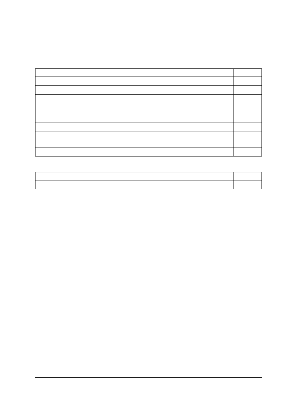
Absolute maximum ratings
Thermal resistance
NOTES:
(a) For a device surface mounted on 25mm x 25mm x 0.6mm FR4 PCB with high coverage of single sided 1oz copper, in
still air conditions.
(b) For device with two active dice running at equal power.
(c) Pulse width <=300
s limit repetition rate to comply with maximum junction temperature.
Parameter
Symbol
Limit
Unit
Supply voltage
V
CC
20
V
Input voltage
V
IN
20
V
I
(sink)PK
9
A
Source current @ I
IN1
+ I
IN2
=10mA
I
(source)
2.2
A
Sink current @ I
IN1
+ I
IN2
=10mA
I
(sink)
2
A
Input current
I
IN1
, I
IN2
1
A
Power dissipation at T
A
=25
°C
Linear derating factor
P
D
1.1
8.8
W
mW/
°C
Operating and storage temperature range
T
j
, T
stg
-55 to +150
°C
Parameter
Symbol
Value
Unit
Junction to ambient
R
JA
113
°C/W
Advertising