Zxld1615 – Diodes ZXLD1615 User Manual
Page 2
ABSOLUTE MAXIMUM RATINGS
(Voltages to GND unless otherwise stated)
Input voltage (V
IN
)
7V
LX output voltage (V
LX
)
30V
Switch output current (I
LX
)
500mA
Power dissipation (PD)
300mW
Operating temperature (T
OP
)
-40 to 85°C
Storage temperature (T
ST
)
-55 to 150°C
Junction temperature (Tj
MAX
)
125°C
ZXLD1615
S E M I C O N D U C T O R S
ISSUE 3 - AUGUST 2004
2
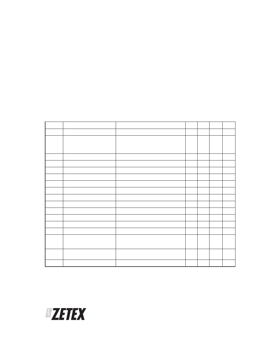
Symbol
Parameter
Conditions
Min
Typ
Max
Units
V
IN
Input voltage
2.5
5.5
V
I
IN
Supply current
Quiescent
Shutdown
V
EN
= V
IN
, I
LX
= 0, Output not switching
V
EN
= 0V
60
<10
100
100
µA
nA
V
FB
FB pin control voltage
0.98
1.07
V
f
LX
Operating frequency
L=10
H, V
OUT
=28V, 5mA load
600
kHz
T
OFF
LX output ‘OFF’ time
350
500
ns
T
ON
(2)
LX output ‘ON’ time
5
µs
I
LXpk
Switch peak current limit
L=10
H, V
OUT
=28V, 5mA load
320
mA
R
LX
Switch 'On' resistance
1.75
⍀
I
LX(leak)
Switch leakage current
V
LX
=20V
1
µA
V
ENH
EN pin high level Input voltage Device active
1.5
V
IN
V
V
ENL
EN pin low level Input voltage
Device in shutdown
0.4
V
I
ENL
EN pin low level input current
V
EN
=0V
-100
nA
I
ENH
EN pin high level input current V
EN
=V
IN
1
A
T
EN(hold)
(3)
EN pin turn off delay
V
EN
switched from high to low
120
µs
⌬T/T
PWM duty cycle range at
‘EN’ input for dc output
voltage control
10kHz < f < 100kHz, V
ENH
=V
IN
20
100
%
f
LPF
Internal PWM low pass filter
cut-off frequency
4
kHz
A
LPF
Filter attenuation
f=30kHz
52.5
dB
ELECTRICAL CHARACTERISTICS:
(Test conditions: V
IN
=V
EN
=3V, T
AMB
=25°C unless otherwise stated
(1)
)
NOTES:
1 Production testing of the device is performed at 25°C. Functional operation of the device over a –40°C to +85°C temperature range is
guaranteed by design, characterization and process control.
2 Nominal ‘on’ time (TONnom ) is defined by the input voltage (V
IN
), coil inductance (L) and peak current (I
LXpkdc
) according to the expression:
T
ONnom
= {I
LX(pkdc)
x L/V
IN
} +200ns
3 This is the time for which the device remains active after the EN pin has been asserted low. This delay is necessary to allow the output to be
maintained during dc PWM mode operation.
4 The maximum PWM signal frequency during this mode of operation should be kept as low as possible to minimize errors due to the turn-off
delay