Adjustable precision shunt regulator, Electrical characteristics – Diodes TL432 User Manual
Page 3
TL431/TL432
ADJUSTABLE PRECISION SHUNT REGULATOR
TL431
*SO-8 is a future package
Document number: DS35044 Rev. 6 - 2
3 of 14
April 2012
© Diodes Incorporated
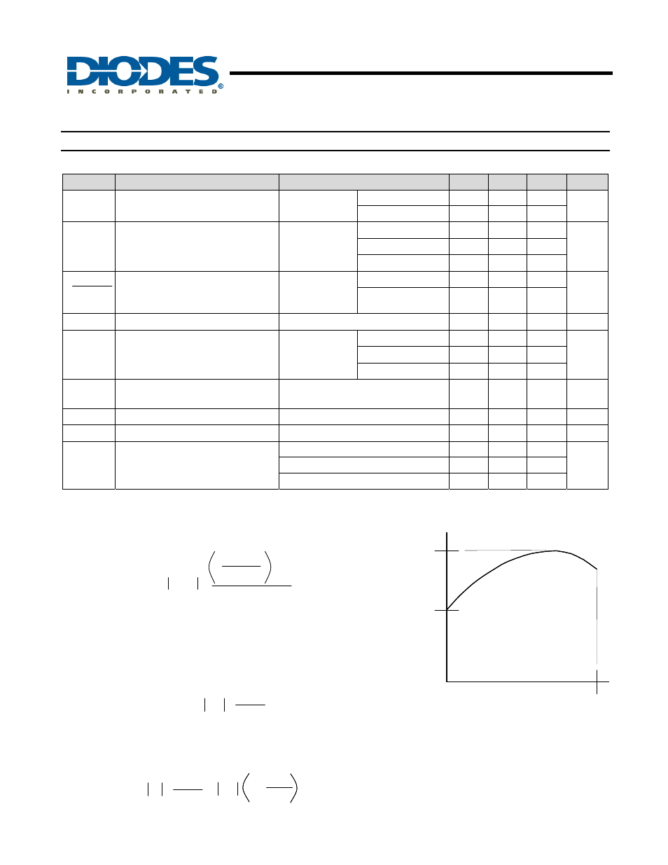
Electrical Characteristics
(T
A
= +25°C, unless otherwise noted)
Symbol
Parameter
Test Conditions
Min
Typ.
Max
Unit
V
REF
Reference voltage
V
KA
= V
REF
,
I
KA
= 10mA
TL431A 2.470
2.495
2.520
V
TL431B 2.482
2.495
2.507
V
DEV
Deviation of reference voltage over
full temperature range (Note 5)
V
KA
= V
REF
,
I
KA
= 10mA
T
A
= 0 to 70
o
C
6
16
mV
T
A
= -40 to +85
o
C
14
34
T
A
= -40 to +125
o
C
14
34
ΔV
REF
ΔV
KA
Ratio of the change in reference
voltage to the change in cathode
voltage
I
KA
= 10mA
V
KA
= 10V to V
REF
-1.4
-2.7
mV/V
V
KA
= 36V to 10V
-1 -2
I
REF
Reference input current
I
KA
= 10mA, R1 = 10K
Ω, R2 = ∞
1 4 µA
ΔI
REF
I
REF
deviation over full temperature
range (Note 7)
I
KA
= 10mA,
R1 = 10K
Ω,
R2 =
∞
T
A
= 0 to 70
o
C
0.8
1.2
µA
T
A
= -40 to +85
o
C
0.8
2.5
T
A
= -40 to +125
o
C
0.8
2.5
I
KA(MIN)
Minimum cathode current for
regulation
V
KA
= V
REF
0.4
0.7
mA
I
KA(OFF)
Off-state current
V
KA
= 36V, V
REF
= 0V
0.05
0.5 µA
|Z
KA
|
Dynamic output impedance (Note 8)
V
KA
= V
REF,
f = 0Hz
0.2
0.5
Ω
θ
JA
Thermal Resistance Junction to
Ambient
SOT23
380
o
C/W
SOT25
250
SO-8*
70
Notes: 7. Deviation of V
DEV
, and
ΔI
REF
are defined as the maximum variation of the values over the full temperature range.
The average temperature coefficient of the reference input voltage
αV
REF
is defined as:
Where:
T2 – T1 = full temperature change.
αV
REF
can be positive or negative depending on whether the slope is
positive or negative.
Notes: 8. The dynamic output impedance, R
Z
, is defined as:
When the device is programmed with two external resistors R1 and R2, the dynamic output
impedance of the overall circuit, is defined as:
=
T2 – T1
αV
REF
V
DEV
V
REF
@ 25ºC
X 10
6
ppm/ºC
=
T2 – T1
αV
REF
V
DEV
V
REF
@ 25ºC
X 10
6
ppm/ºC
Vmax
Vmin
T1
T2
V
DEV
= Vmax - Vmin
Temperature
Vmax
Vmin
T1
T2
V
DEV
= Vmax - Vmin
Temperature
=
Z
KA
ΔV
KA
ΔI
KA
=
Z
KA
ΔV
KA
ΔI
KA
=
Z’
ΔV
ΔI
Z
KA
1 +
R1
R2
≈
=
Z’
ΔV
ΔI
=
Z’
ΔV
ΔI
Z
KA
1 +
R1
R2
Z
KA
1 +
R1
R2
≈