Altera Cyclone II PowerPlay Early Power Estimator User Manual
Page 30
3–14
Altera
Corporation
PowerPlay Early Power Estimator User Guide For Cyclone II FPGAs
May 2006
PowerPlay Early Power Estimator Spreadsheet Inputs
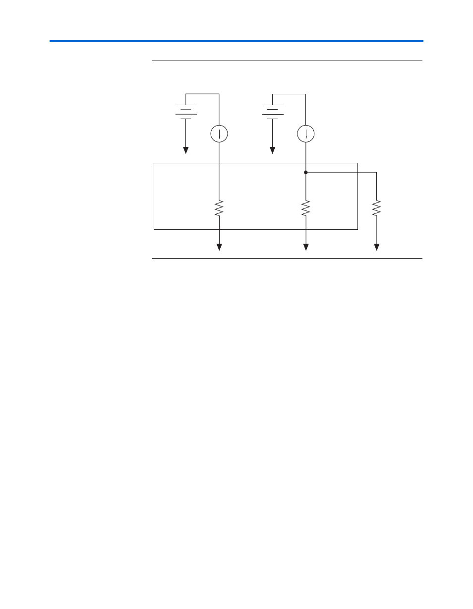
Figure 3–10. I/O Power Representation
The V
REF
pins consume minimal current (less than 10
μA) and is
negligible when compared to the power consumed by the general
purpose I/O pins. Therefore, the PowerPlay Early Power Estimator
spreadsheet does not include the current for V
REF
pins in the calculations.
Each row in the I/O section represents a design module where the I/O
pins have the same frequency, toggle percentage, average capacitive load,
I/O standard, data rate, and I/O bank. You must enter the following
parameters for each design module:
■
I/O standard
■
Clock frequency (f
MAX
) in MHz
■
Number of output, input, and bidirectional pins
■
I/O bank
■
Pin toggle percentage
■
Output enable percentage
■
Average capacitance of the load
■
I/O data rate
V
CCINT
V
CCIO
I
CCINT
I
CCIO
Thermal P
INT
Thermal P
IO
External P
IO
Cyclone II Device