Altera Internal Memory (RAM and ROM) IP Core User Manual
Page 51
Ports Name
Ports
Type
Descriptions
address_a
data_a
wren_a
rden_a
Input
Address input, data input, write enable, and read enable to
port A of the RAM.
(17)
address_b
data_b
wren_b
rden_b
Input
Address input, data input, write enable, and read enable to
port B of the RAM.
(17)
rdata1
err_corrected1
err_detected1
err_fatal1
Output Output data read from port A of the RAM, and the ECC-
status signals reflecting the data read.
(18)
rdata2
err_corrected2
err_detected2
err_fatal2
Output Output data read from port B of the RAM, and the ECC-
status signals reflecting the data read.
(18)
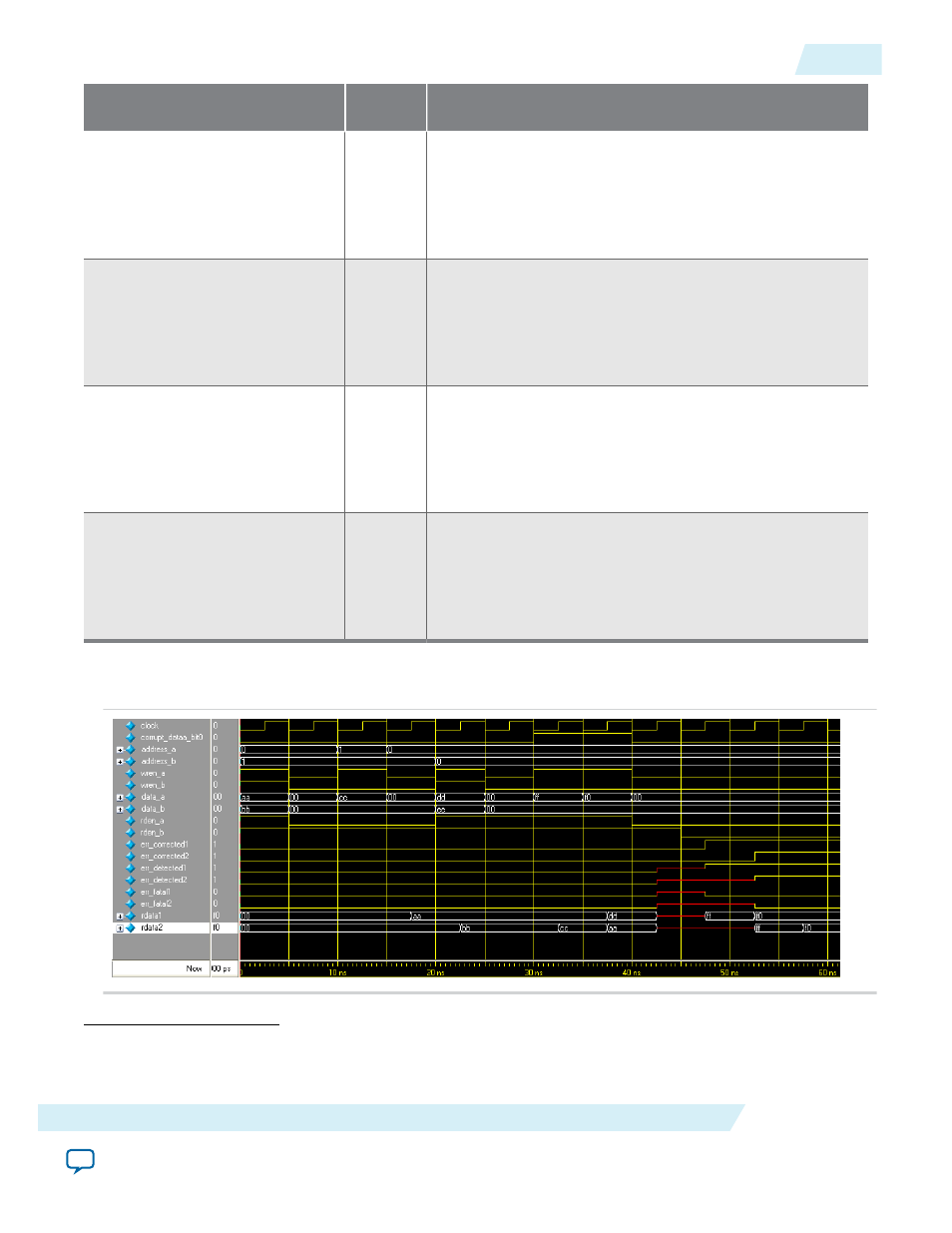
Figure 5-1: Simulation Results
This figure shows the expected simulation waveform results in the ModelSim-Altera software.
(18)
The encoder and decoder each use one pipeline while the RAM uses two pipelines, making the total
pipeline equal to four. Therefore, read data is only shown at output ports four clock cycles after the read
enable is initiated.
UG-01068
2014.12.17
Simulation Results
5-5
Design Example
Altera Corporation