Altera PowerPlay Early Power Estimator User Manual
Page 25
Chapter 3: Using Cyclone III PowerPlay Early Power Estimator
3–13
PowerPlay Early Power Estimator Inputs
© June 2009 Altera Corporation
PowerPlay Early Power Estimator User Guide for Cyclone III FPGAs
Table 3–5
describes the I/O power rail information in the I/O section of the PowerPlay
Early Power Estimator.
Table 3–6
describes the parameters in the I/O section of the PowerPlay Early Power
Estimator.
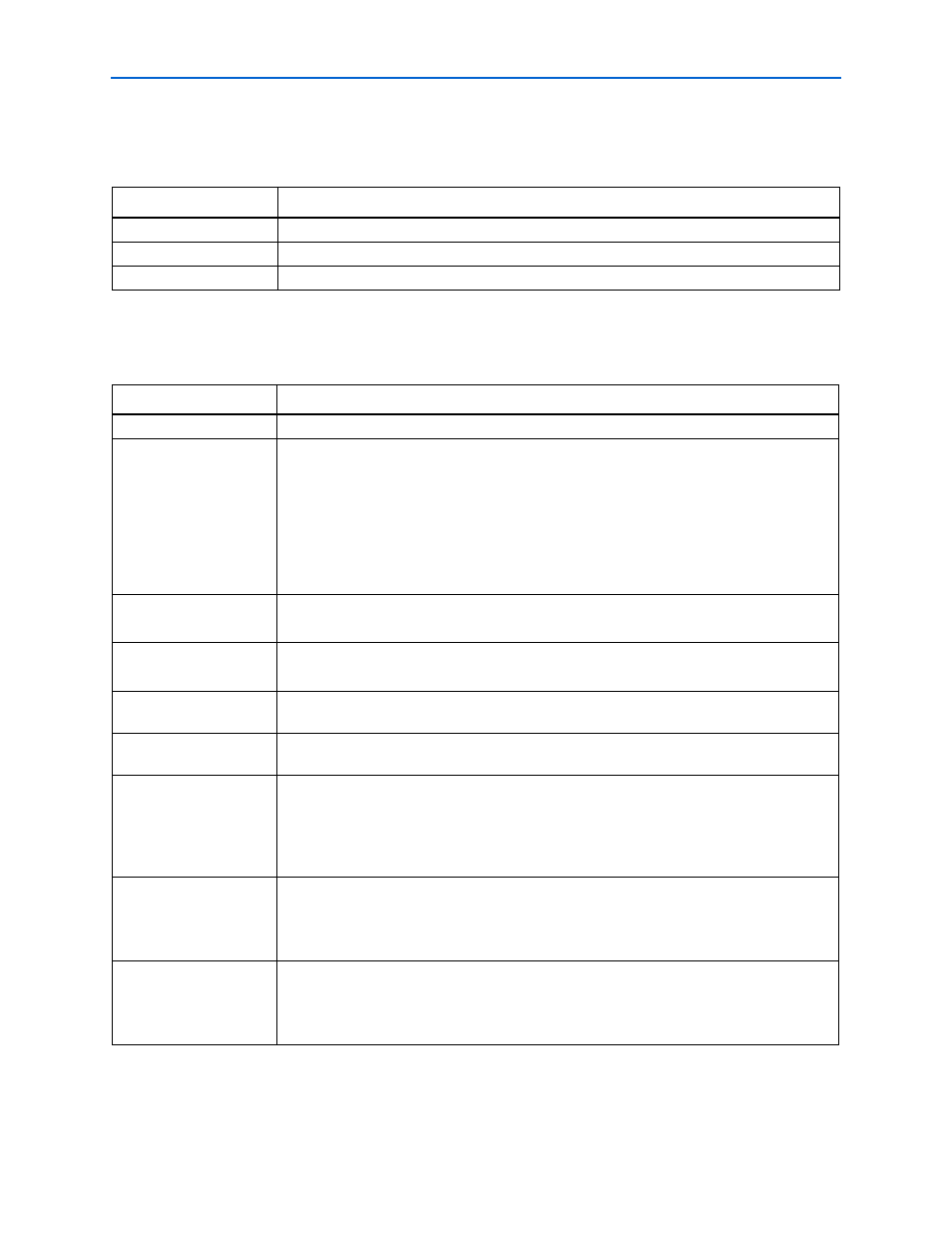
Table 3–5. I/O Power Rail Information in the I/O Section
Parameter
Description
Power Rails
Power supply rails for the I/O pins
Voltage (V)
The voltage applied to the specified power rail in Volts (V)
Current (A)
The current drawn from the specified power rail in Amps (A)
Table 3–6. I/O Section Information (Part 1 of 2)
Parameter
Description
Module
Enter a name for the module in this column. This is an optional value.
I/O Standard
Select the I/O standard used for the input, output, and bidirectional pins in this module from
the list.
The calculated I/O power varies based on the I/O standard. For I/O standards that recommend
termination (SSTL and HSTL), the PowerPlay Early Power Estimator assumes that you are
using external termination resistors. If you are not using external termination resistors, Altera
recommends that you choose the LVTTL/LVCMOS I/O standard with the same voltage as the
terminated I/O standard. There are up and down scroll bars to view all the I/O standards in the
pull-down list.
Current Strength/
Output Termination
Select the current strength or output termination implemented for the I/O pin or pins in this
module. Current strength and output termination are mutually exclusive.
Slew Rate
Select the slew rate setting for the output and bidirectional pin or pins in this module.
Using a lower slew rate setting helps reduce switching noise but may increase delay.
# Input Pins
Enter the number of input pins used in this module. A differential pair of pins should be
considered as one pin.
# Output Pins
Enter the number of output pins used in this module. A differential pair of pins should be
considered as one pin.
# Bidir Pins
Enter the number of bidirectional pins used in this module. The I/O pin is treated as an output
when its output enable signal is active and an input when the output enable is disabled.
An I/O pin configured as bidirectional but used only as an output consumes more power than
one configured as output-only, due to the toggling of the input buffer every time the output
buffer toggles (they share a common pin).
Data Rate
Select either SDR or DDR as the I/O data rate.
This indicates whether the I/O value is updated once (SDR) or twice (DDR) a cycle. If the data
rate of the pin is DDR, it is possible to set the data rate to SDR and double the toggle
percentage. The Quartus II software often uses this method to output information.
Clock Freq (MHz)
Enter the clock frequency (in MHz). This value is limited by the maximum frequency
specification for the device family.
100 MHz with a 12.5% toggle rate means that each I/O pin toggles 12.5 million times per
second (100 × 12.5%).