Video decoder interface, Hc_ps2_clk, Ps2_clk – Altera LCD Multimedia HSMC User Manual
Page 31: Hc_ps2_dat, Ps2_dat
2–23
Altera Corporation
LCD Multimedia HSMC
August 2008
Interfaces/ Connectors
shows the pinout of PS/2 Interface with HSMC connector.
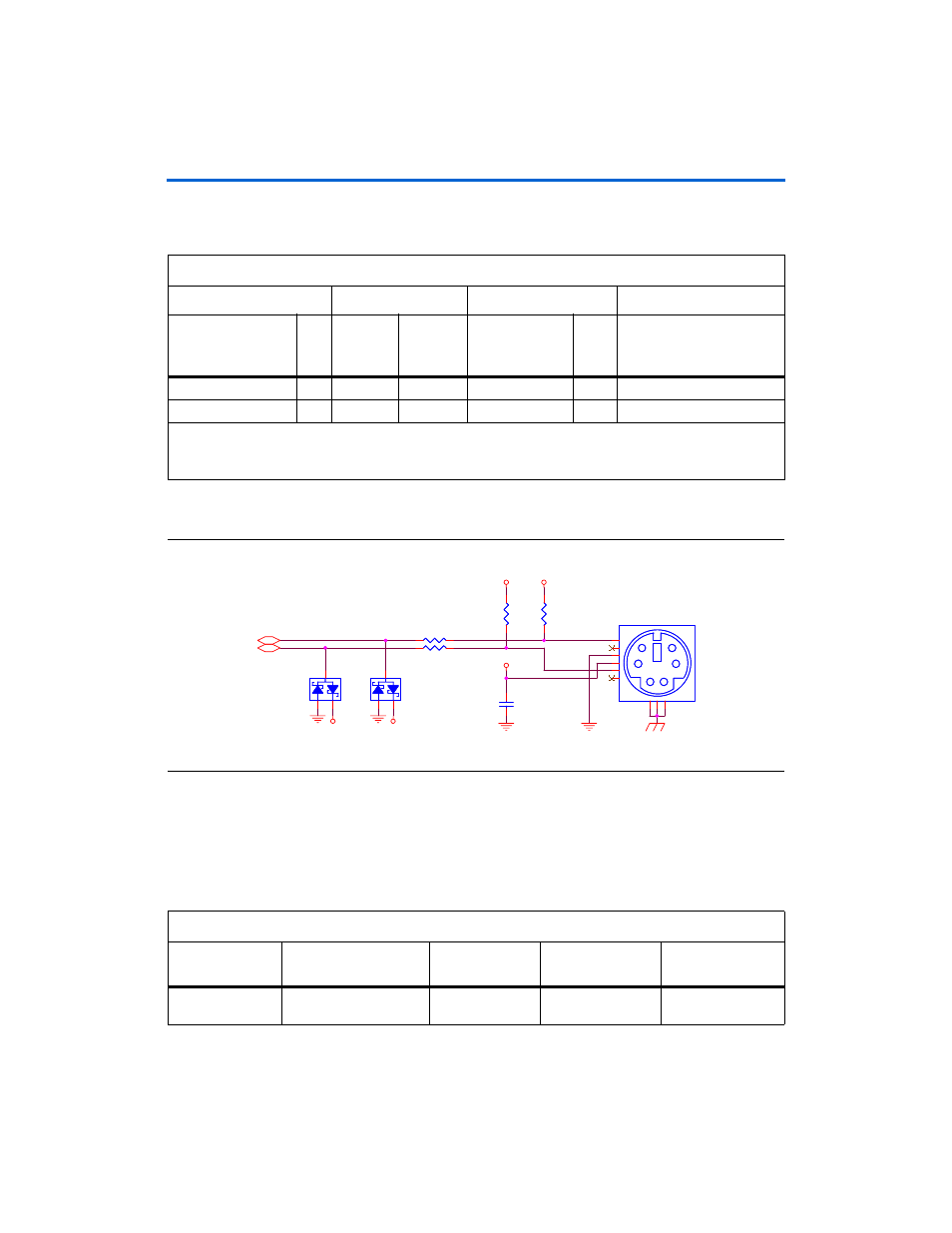
shows the PS/2 interface schematic.
Figure 2–13. PS/2 Interface Schematic
Video Decoder Interface
The board is equipped with an Analog Devices ADV7180 Video decoder
chip and RCA input jack (J11).
below lists Video Decoder
Interface board reference and manufacturing information.
Table 2–16. PS/2 Interface Pinout with HSMC Connector
HSMC Connector
MAX II
PS/2 Interface
Signal Name
Pin
No.
HSMC
Connector
Side Pin
Device
Side Pin
Signal Name
Pin
No.
Description
HC_PS2_CLK
43
U10-3
(
U10-12
)
PS2_CLK
1
PS/2 Clock
HC_PS2_DAT
47
U10-4
(
U10-11
)
PS2_DAT
6
PS/2 Data
Notes:
(1)
These signals do not go through the MAX II chip. They pass through the MAX3378 level translator chip, U10.
PS2CLK
PS2DAT
PS2_DAT
PS2_CLK
VCC5
VCC5
VCC33
VCC33
VCC5
R56
120
R56
120
BC34
0.1U
BC34
0.1U
3
5
TOP
8
6
2
1
J9
PS2
3
5
TOP
8
6
2
1
J9
PS2
3
5
6
9
10
11
2
1
8
R55
120
R55
120
R53
2K
R53
2K
D3
BAT54S
D3
BAT54S
1
2
3
R54
2K
R54
2K
D4
BAT54S
D4
BAT54S
1
2
3
Table 2–17. Video Decoder Interface
Board Reference
Device Description
Manufacturer
Manufacturer Part
Number
Manufacturer
Website
U8
10-Bit, 4× Oversampling
SDTV Video Decoder
Analog Devices
ADV7180