Altera Stratix III Development Board User Manual
Page 70
2–62
Chapter 2: Board Components
On-Board Memory
Stratix III 3SL150 Development Board
May 2013
Altera Corporation
Reference Manual
lists the Samsung device latency values based on operation frequency.
show the Samsung device read and write access
waveforms.
Table 2–53. SRAM Latency Vs. Frequency
Item
Up to 66 MHz
Up to 80 MHz
Up to 104 MHz
Fixed
Variable
Fixed
Variable
Fixed Variable
Latency set (A11:A10:A9)
4(0:0:1)
2(1:0:0)
5(0:1:0)
3(0:0:0)
7(1:0:1)
4(0:0:1)
Read latency (min)
4
2/4
5
3/5th
7
4/7
First read data fetch clock
5th
3rd/5th
6th
4th/6th
8th
5th/8th
Write latency (min)
2
2
3
3
4
4
First write data loading clock
3rd
3rd
3rd
4th
5th
5th
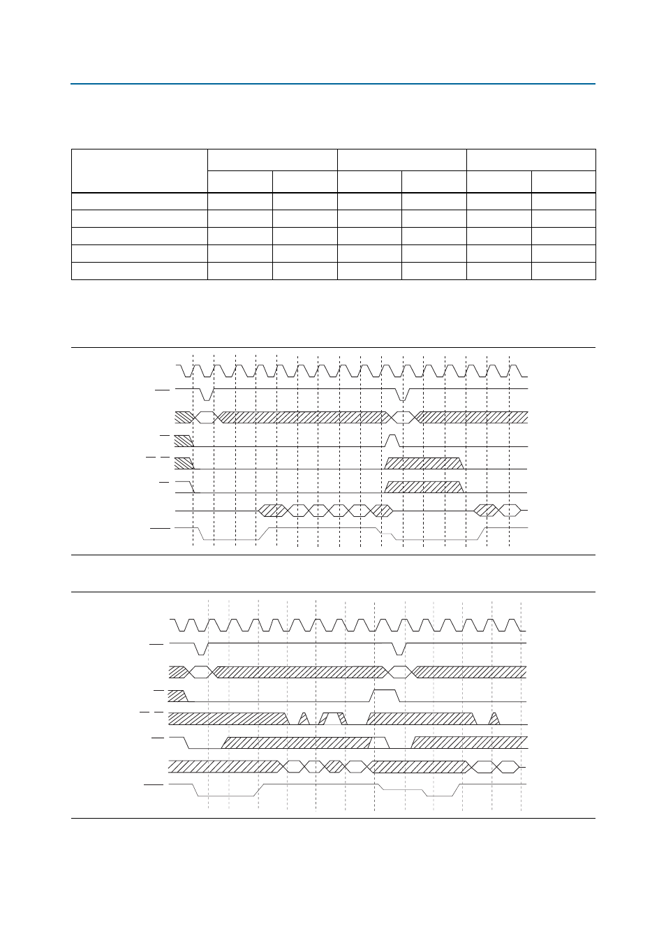
Figure 2–18. SRAM Read Timing Waveforms
0
1
2
3
4
5
6
7
8
9
10
11
12
13
14
Data Out
OE
ADDR
ADV
CLK
WAIT
CS
UB, LB
Figure 2–19. SRAM Write Timing Waveforms
0
1
2
3
4
5
6
7
8
9
10
11
12
13
14
Data In
WE
UB, LB
CS
ADDR
ADV
CLK
WAIT