Block diagram, Handling the board, Block diagram –4 – Altera Stratix III Development Board User Manual
Page 8: Handling the board –4
1–4
Chapter 1: Overview
Handling the Board
Stratix III 3SL150 Development Board
May 2013
Altera Corporation
Reference Manual
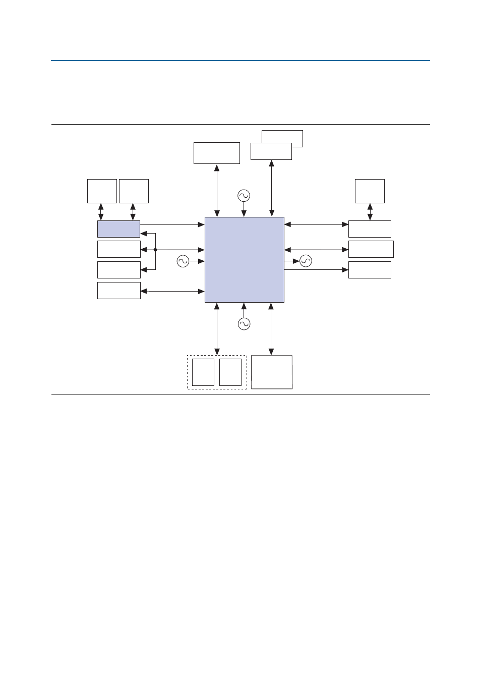
Block Diagram
shows the functional block diagram of the Stratix III development board.
Handling the Board
When handling the board, it is important to observe the following precaution:
c
Static Discharge Precaution: Without proper anti-static handling, the board can be
damaged. Therefore, use anti-static handling precautions when touching the board.
Figure 1–1. Stratix III Development Board Block Diagram
1.5-V HSTL
Statix III
EP3SL1501152
EP3SL340H1152
125-MHz
XTAL
MAX II
Device (x16)
2.5-V CMOS
1.8-V CMOS
Power
Measure/
Display
72-Mbit QDRII/+
18/18
CMOS + LVDS
4-MB SSRAM
(x32)
64-MB Flash
(x16)
1-GByte DDR2
(x72)
USB
2.0
1.8-V SSTL
50-MHz
XTAL
1.8-V CMOS
Quad 7-Seg/
User LEDs,
Buttons,
Switches
SMA Input
1.8-V SSTL
SMA Output
10/100/1000
Ethernet
CMOS + LVDS
2.5-V CMOS
RJ45
Jack
Graphics Display
Header
14-Pin LCD
Header
16-MB
DDR2
(x8)
16-MB
DDR2
(x8)
HSMC Port B
HSMC Port A