Foxconn 915P7AD-8EKRS User Manual
Page 59
Chapter 3 BIOS Description
5 2
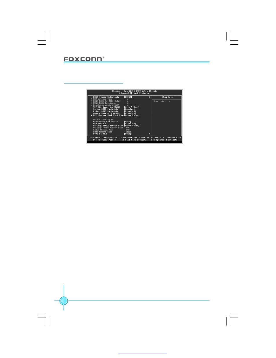
Advanced Chipset Features
v
DRAM Timing Selectable (Default: By SPD)
This item determines DRAM clock/ timing using SPD or manual configuration.
The available setting values are: By SPD and Manual.
v
CAS Latency Time (Default: depend on memory)
This item determines CAS Latency. The available setting values are: 3, 2.5, 2
and Auto.
v
DRAM RAS# to CAS# Delay (Default: depend on memory)
This item allows you to select a delay time between the CAS and RAS strobe
signals. The available setting values are: 5, 4, 3, 2, and Auto.
v
DRAM RAS# Precharge (Default: depend on memory)
This item allows you to select the DRAM RAS# precharge time. The available
setting values are: 5, 4, 3, 2, and Auto.
v
Precharge delay(tRAS) (Default: depend on memory)
This item allows you to set the precharge delay time. The available setting
values are: Auto, 4 - 15.
v
SLP_S4# Assertion Width (Default: 4 to 5 Sec.)
This option indicates the assertion width of the SLP_S4# signal to guarantee
that the DRAMs have been safely power-cycled. The available setting values
are: 1 to 2 sec., 2 to 3 sec., 3 to 4 sec., 4 to 5 sec. .
Advanced Chipset Features Menu
PDF created with pdfFactory Pro trial version