IBASE SI-38 User Manual
Page 20
Advertising
20
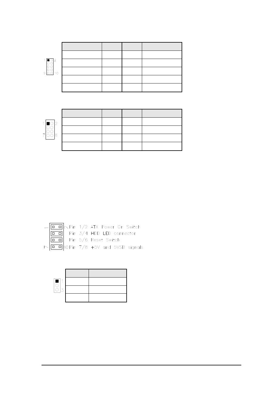
J9: Digital I/O
Signal Name
Pin #
Pin #
Signal Name
GND
1
2
VCC
OUT3
3
4
OUT1
OUT2
5
6
OUT0
IN3
7
8
IN1
IN2
9
10
IN0
JP10: US2.0 Connector
Signal Name
Pin #
Pin #
Signal Name
Vcc
1
2
Ground
D-
3
4
D+
D+
5
6
D-
Ground
7
8
Vcc
J12: Mini PCIE Slot (Support mSATA)
J17: MCU JTAG (factory use only)
J19: Power LED Connector
J20: System Function Connector
J19: Power LED Connector
Pin #
Signal Name
1
+5V
2
NC
3
Ground
Advertising
See also other documents in the category IBASE Computers:
- IPPC08A7 (70 pages)
- IB898 (58 pages)
- IB908 (76 pages)
- IB906 (56 pages)
- IB520 (56 pages)
- IB550 (58 pages)
- IB893 (68 pages)
- IB892 (56 pages)
- IB905 (62 pages)
- IB882 (56 pages)
- IB903 (58 pages)
- IB886 (60 pages)
- IB889 (56 pages)
- IB897 (64 pages)
- IB885 (58 pages)
- IB530 (56 pages)
- IB950 (63 pages)
- IB825 (68 pages)
- IB815 (63 pages)
- IB704 (51 pages)
- AMS100-807 (12 pages)
- AMI400 (27 pages)
- CSB200-888 (13 pages)
- SI-06 (44 pages)
- SI-22 (51 pages)
- SI-18 (51 pages)
- IOPS-76 (36 pages)
- SI-28 (44 pages)
- SI-606 (103 pages)
- SI-12 (48 pages)
- SI-304 (62 pages)
- SI-32-N (50 pages)
- SI-62 (73 pages)
- SI-64 (80 pages)
- SE-92 (63 pages)
- SI-83 (78 pages)
- SI-38N (53 pages)
- IOPS-18 (46 pages)
- SI-58 (73 pages)
- IPPCXXA7-RE (59 pages)
- INOSP Series (74 pages)
- IPPC15B7-RE (55 pages)
- MRS-801-RE (94 pages)
- SSPA-24 (7 pages)