0 control & data registers – Measurement Computing PC104-DAC06 User Manual
Page 11
If frequent changes to signal connections or signal conditioning are required, please
refer to the information on the CIO-TERMINAL, CIO-SPADE50, CIO-MINI40 and
CIO-MINI37 (if using a BP40-37 adapter) screw terminal boards.
Figure 3-4. Board Connector
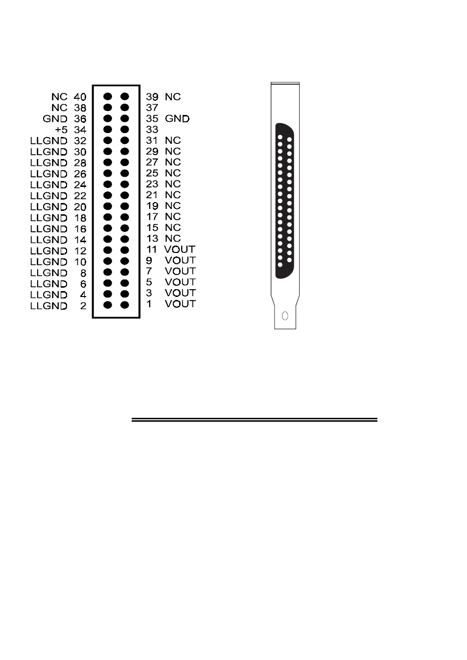
Figure 3-5 Cable BP40-37 Pin-Out
4.0 CONTROL & DATA REGISTERS
All control and data is read/written with simple I/O read and write signals. No
interrupt or DMA control software is required. Hence, the board's functions are easy
to control directly from BASIC, C or PASCAL.
The PC104-DAC06 has 12 analog output registers. There are two for each channel,
one for the lower eight bits and one for the upper four bits.
The first address, or BASE ADDRESS, is determined by setting a bank of switches on
the board.
A register is easy to read and write to. The register descriptions all follow the format:
7
-12VDC
+12VDC
0
1
2
3
4
5
37 GND
36 +5VDC
35 LLGND
34 LLGND
33 LLGND
32 LLGND
31 LLGND
30 LLGND
29 LLGND
28 LLGND
27 LLGND
26 LLGND
25 LLGND
24 LLGND
23 LLGND
22 LLGND
21 LLGND
20 LLGND
–12VDC 19
GND 18
+12VDC 17
NC 16
NC 15
NC 14
NC 13
NC 12
NC 11
NC 10
NC 9
NC 8
NC 7
6
5
VOUT 3 4
3
2
VOUT 0 1
VOUT 1
VOUT 2
VOUT 4
VOUT 5