Analog output calibration, Digital input/output – Measurement Computing USB-3102 User Manual
Page 22
USB-3102 User's Guide
Specifications
22
Note 5:
Each of the four DAC8554 outputs controls a VOUTx and IOUTx channel-pair simultaneously.
So, for example, when writing to channel VOUT0, the associated IOUT0 channel will also be
updated. Conversely, when writing to channel IOUT0, the associated VOUT0 channel is also
updated. Unused VOUTx and IOUTx output channels should be left disconnected.
Note 6:
The following formula will calculate the maximum load resistance for correct IOUT circuit
operation. The compliance voltage applied should not exceed the limits specified in Table 5.
Calibrated Output:
Load Resistance = (Compliance Voltage - 6V)/0.020A
Un-Calibrated Output:
Load Resistance = (Compliance Voltage - 6V)/0.025A
Note 7:
The maximum differential non-linearity specification applies to the entire 0 to 70 °C temperature
range of the USB-3102. This specification also accounts for the maximum errors due to the
software calibration algorithm (in Calibrated mode only) and the DAC8554 digital to analog
converter non-linearities.
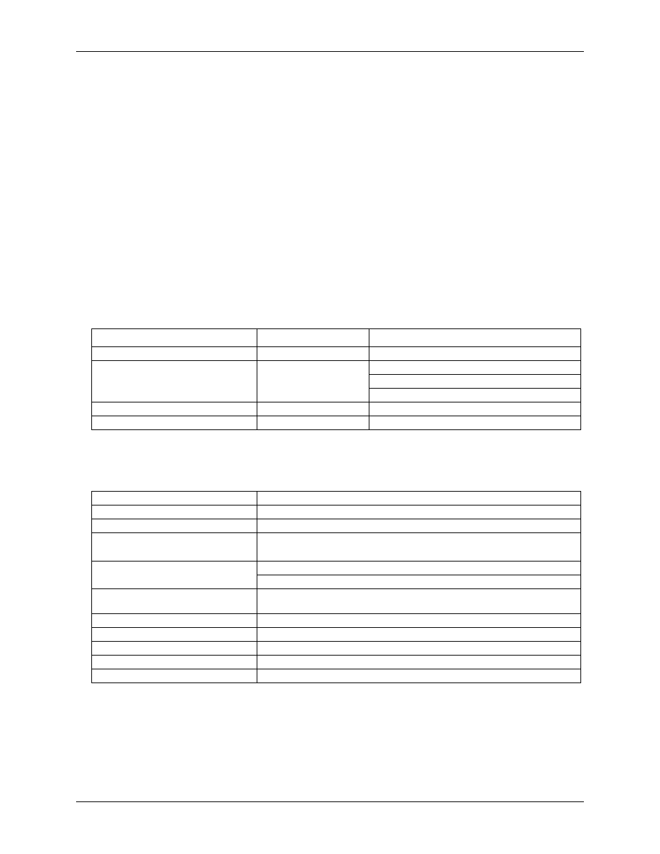
Analog output calibration
Table 6. Analog output calibration specifications
Parameter
Conditions
Specifications
Recommended warm-up time
15 minutes min.
On-board precision reference
DC level: 5.000 V ±1 mV max.
Tempco: ±10 ppm/°C max.
Long term stability: ±10 ppm/SQRT(1000 hrs)
Calibration method
Software calibration
Calibration interval
1 year
Digital input/output
Table 7. Digital I/O specifications
Digital logic type
CMOS
Number of I/O
8
Configuration
Independently configured for input or output
Pull-up/pull-down configuration
(Note 8)
User configurable
All pins floating (default)
Digital I/O input loading
TTL (default)
47K ohms (pull-up/pull down configurations)
Digital I/O transfer rate (system paced)
System dependent, 33 to 1000 port reads/writes or single bit reads/writes per
second.
Input high voltage
2.0 V min, 5.5 V absolute max
Input low voltage
0.8 V max, –0.5 V absolute min
Output high voltage (IOH = –2.5 mA)
3.8 V min
Output low voltage (IOL = 2.5 mA)
0.7 V max
Power on and reset state
Input
Note 8:
Pull up and pull down configuration area available using the DIO CTL terminal block pin 54.
The pull down configuration requires the DIO CTL pin (pin 54) to be connected to a DGND pin
(pin 50, 53 or 55). For a pull up configuration, the DIO CTL pin should be connected to the +5V
terminal pin (pin 56).