Outline description, Figure 3: block diagram – Sundance SMT317 User Manual
Page 7
Advertising
Version 6.1
Page 7 of 24
SMT317 User Manual
4.
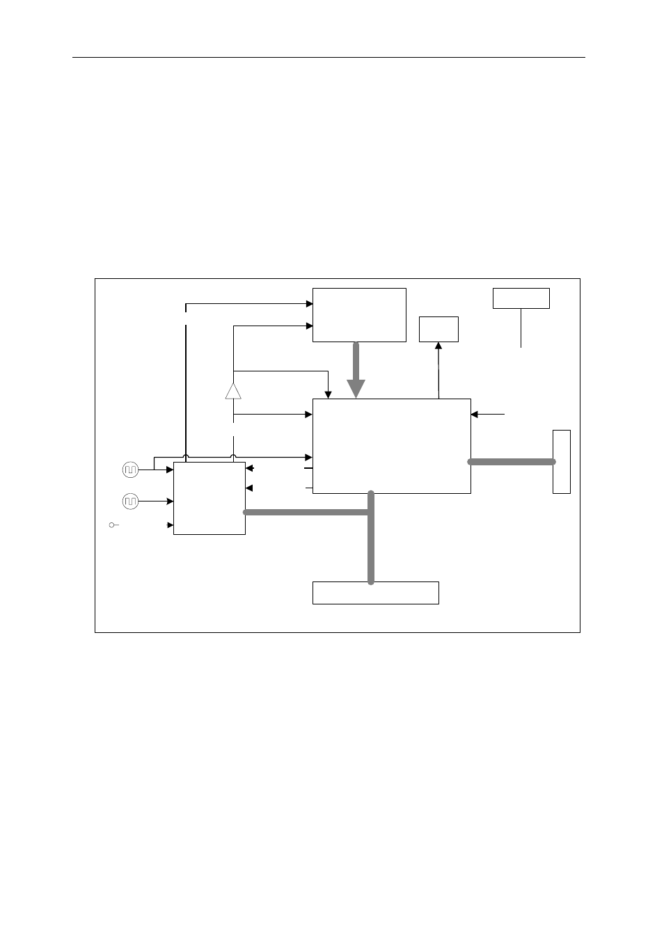
Outline Description
The SMT317v2 module is an ADC-based size 1 TIM offering the following features:
• Eight 16-bits ADCs running at an output word rate of up to 1.2 MHz for input
bandwidths up to 460 kHz.
• a Xilinx XCV300 Virtex FPGA.
• FPGA programming via communication port (comm-port3).
• High bandwidth data I/O via 1 Sundance Digital Bus (SDB).
VIRTEX
ADC SUB-SYSTEM
S
D
B
4 LEDs
4 I/Os
JUMPERS
CONFIG CPLD
on Comm-port3
Local clock
37.6 MHz
PRIMARY
1 SDB
Comm-port 3
External clock
Clock Buffer
Sample clock
Clock select
SYNC
External SYNC
8 A
D
C
s
Cl
ock
Co
nt
ro
l Co
mm-po
rt
s
e
le
c
tion
Internal sync
C
o
m
m
-por
t 3
Figure 3: Block Diagram
Advertising