Sundance SMT712 User Manual
Page 23
User Manual SMT712
Page 23 of 89
Last Edited: 11/12/2012 10:36:00
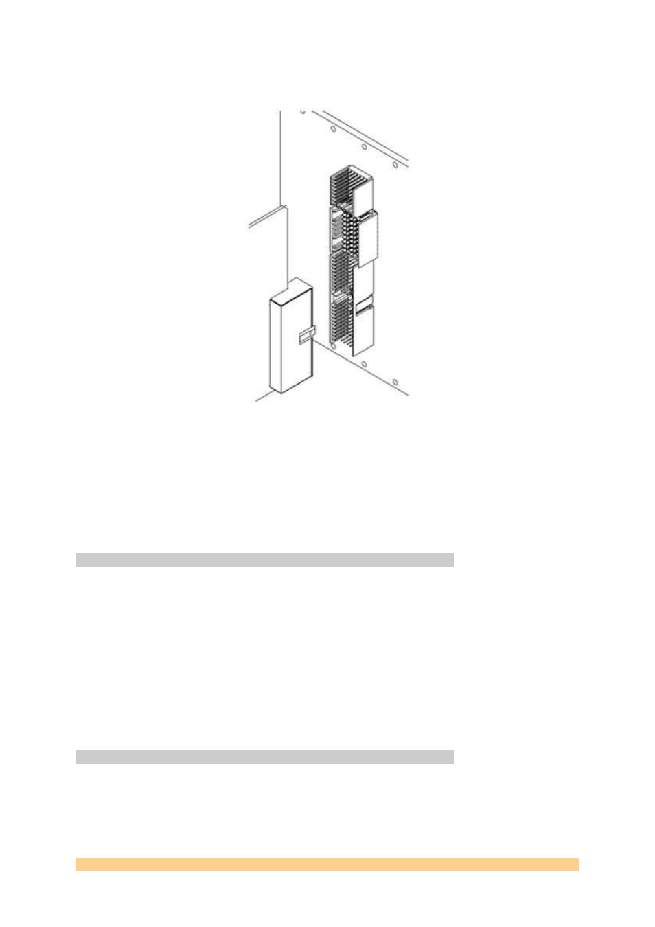
The SMT712 module can also be a 3U Compact PCI module, which can only be
plugged into a CPCI system. It only has one connector fitted: P1 (32-bit, 33MHz PCI
signals).
Figure 10 - SMT712-CPCI32 - Compact PCI Module
The FPGA requires a reference clock to implement either the PCI or PCI Express
core. The selection is made via J11. The Jumper should be fitted in Position1-2 when
a PCI core is used (a 250MHz clock is then available to the FPGA) or in Position2-3
when a PCI Express core is used (the 100-MHz express reference is then routed to
the FPGA).
4.5.8
SHB connector
An SHB (1) Connector is available from the FPGA. It maps 32 single-ended data lines
and a set of control signals including a clock.
It can be used to transfer samples from an other Sundance module, for instance the
SMT702.
A second SHB (2) connector is also available on non-PCI versions of the board.
As an example, both SHBs can be used to link an SMT702 and an SMT712 to create a
dual-channel, 2GSPS PXIe platform.
SHB clock should match the FPGA clock rate used for DAC (clk/8) and SHB data is
automatically phase shifted to be aligned with internal clock.
4.5.9
External Trigger.
The external trigger function is not implemented in current version of the default
firmware.