9 cable diagrams, Terminal block - cn13 i/o, 1 cbk-u-mp2b-xx – Yaskawa SigmaLogic User Manual
Page 31
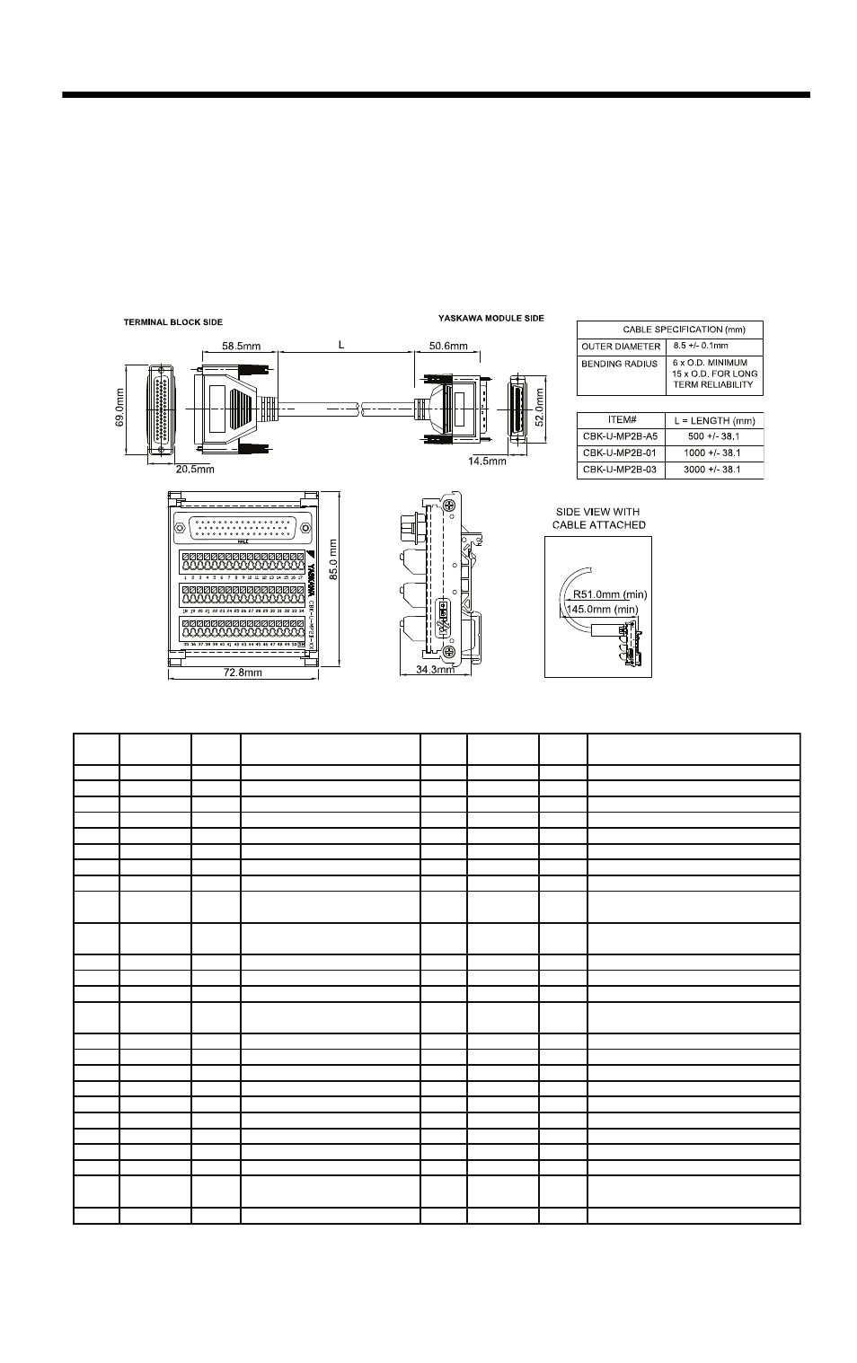
9.1 CBK-U-MP2B-xx
29
9 Cable
Diagrams
9.1 CBK-U-MP2B-xx
Terminal Block - CN13 I/O
CBK-U-MP2B-XX Function Chart for SigmaLogic
I = Input, O = Output, P = Power
Pin
No.
Signal
Name
I/O
Function
Pin
No.
Signal
Name
I/O
Function
1
26
2
27
3
-
-
-
28
reserved
-
4
PA+
I
Phase A pulse (+)
29
PB+
I
Phase B pulse (+)
5
PA-
I
Phase A pulse (-)
30
PB-
I
Phase B pulse (-)
6
GND
P
Encoder input ground
31
GND
P
Encoder input ground
7
BAT+
P
Controller SRAM Battery (+)
32
BAT-
P
Controller SRAM Battery (-)
8
-
-
-
33
-
-
-
-
-
-
9
34
10
35
11
DO_00-
O
Digital output 0 (-)
36
DO_01-
O
Digital output 1 (-)
12
DO_02-
O
Digital output 2 (-)
37
DO_03-
O
Digital output 3 (-)
13
DICOM
I
Digital input common
38
DICOM
I
Digital input common
14
DI_00
I
Digital input 0
39
DI_01
I
Digital input 1
(shared with pulse latch input)
15
DI_02
I
Digital input 2
40
DI_03
I
Digital input 3
16
DI_04
I
Digital input 4
41
DI_05
I
Digital input 5
17
DI_06
I
Digital input 6
42
DI_07
I
Digital input 7
18
DO_04-
O
Digital output 4 (-)
43
DO_05-
O
Digital output 5 (-)
19
DO_06-
O
Digital output 6 (-)
44
DO_07-
O
Digital output 7 (-)
20
-
-
-
45
-
-
-
21
DO_00+
O
Digital output 0 (+)
46
DO_01+
O
Digital output 1 (+)
22
DO_02+
O
Digital output 2 (+)
47
DO_03+
O
Digital output 3 (+)
23
DO_04+
O
Digital output 4 (+)
48
DO_05+
O
Digital output 5 (+)
24
DO_06+
O
Digital output 6 (+)
49
DO_07+
O
Digital output 7 (+) (shared with
position agreement 'COIN' signal)
25
-
-
-
50
-
-
-
-
-
-
-
-
-
-
-
-
-
-
-
-
-
-
-
-
-
-
-
-
-
-
-