Theory of operation, The data input, Using the pdn line – Linx Technologies TXM-xxx-LR User Manual
Page 7
– –
– –
8
9
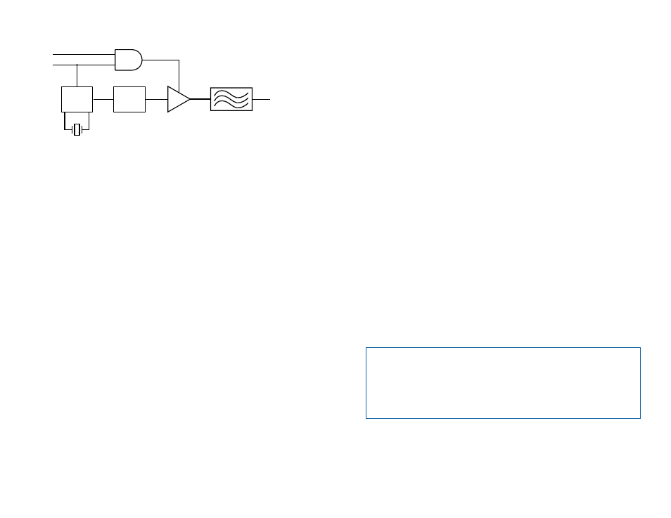
Theory of Operation
The LR Series transmitter generates 1mW of output power into a 50-ohm
single-ended antenna while suppressing harmonics and spurious emissions
to within legal limits. The transmitter is comprised of a VCO locked by a
frequency synthesizer that is referenced to a high precision crystal. The
output of the VCO is amplified and buffered by an internal power amplifier.
The amplifier is switched by the incoming data to produce a modulated
carrier. The carrier is filtered to attenuate harmonics and then output on the
50
Ω antenna port.
The synthesized topology makes the module highly immune to the
effects of antenna port loading and mismatch. This reduces or eliminates
frequency pulling, bit contraction, and other negative effects common to
low-cost transmitter architectures. It also allows for reliable performance
over a wide operating temperature range. Like its companion LR Series
receiver, the LR Series transmitter delivers a significantly higher level of
performance and reliability than the LC Series or other SAW-based devices,
yet remains very small and cost-effective.
PLL
VCO
PA
XTAL
DATA
PDN
RF OUT
The Data Input
The CMOS-compatible data input on Pin 2 is normally supplied with a serial
bit stream from a microprocessor or encoder, but it can also be used with
standard UARTs.
When a logic ‘1’ is present on the DATA line and the PDN line is high, then
the Power Amplifier (PA) is activated and the carrier frequency is output on
the antenna port. When a logic ‘0’ is present on the DATA line or the PDN
line is low, the PA is deactivated and the carrier is fully suppressed.
The DATA line should always be driven with a voltage that is common
to the supply voltage present on Pin 7 (V
CC
). The DATA line should never
be allowed to exceed the supply voltage, as permanent damage to the
module could occur.
Using the PDN Line
The transmitter’s Power Down (PDN) line can be used to power down the
transmitter without the need for an external switch. It allows easy control of
the transmitter’s state from external components, such as a microcontroller.
By periodically activating the transmitter, sending data, then powering
down, the transmitter’s average current consumption can be greatly
reduced, saving power in battery operated applications.
The PDN line does not have an internal pull-up, so it needs to be pulled
high or tied directly to V
CC
to turn on the transmitter. The pull-up should be
a minimum of 30μA (10k
Ω or less). When the PDN line is pulled to ground,
the transmitter enters a low-current (<5nA) power-down mode. In this
mode, the transmitter is completely off and cannot perform any function.
Figure 10: LR Series Transmitter Block Diagram
Note:
The voltage on the PDN line should not exceed V
CC
. When used
with a higher voltage source, such as a 5V microcontroller, an open
collector line should be used or a diode placed in series with the control
line (anode toward the module). Either method avoids damage to the
module by preventing 5V from being placed on the PDN line while
allowing the line to be pulled low.