Rise and fall time test conditions, Scsi input filtering, Figure 3.4 – Avago Technologies LSI53C120 User Manual
Page 43
Electrical Characteristics
3-13
shows the rise and fall time test conditions described in
Figure 3.3
Rise and Fall Time Test Conditions
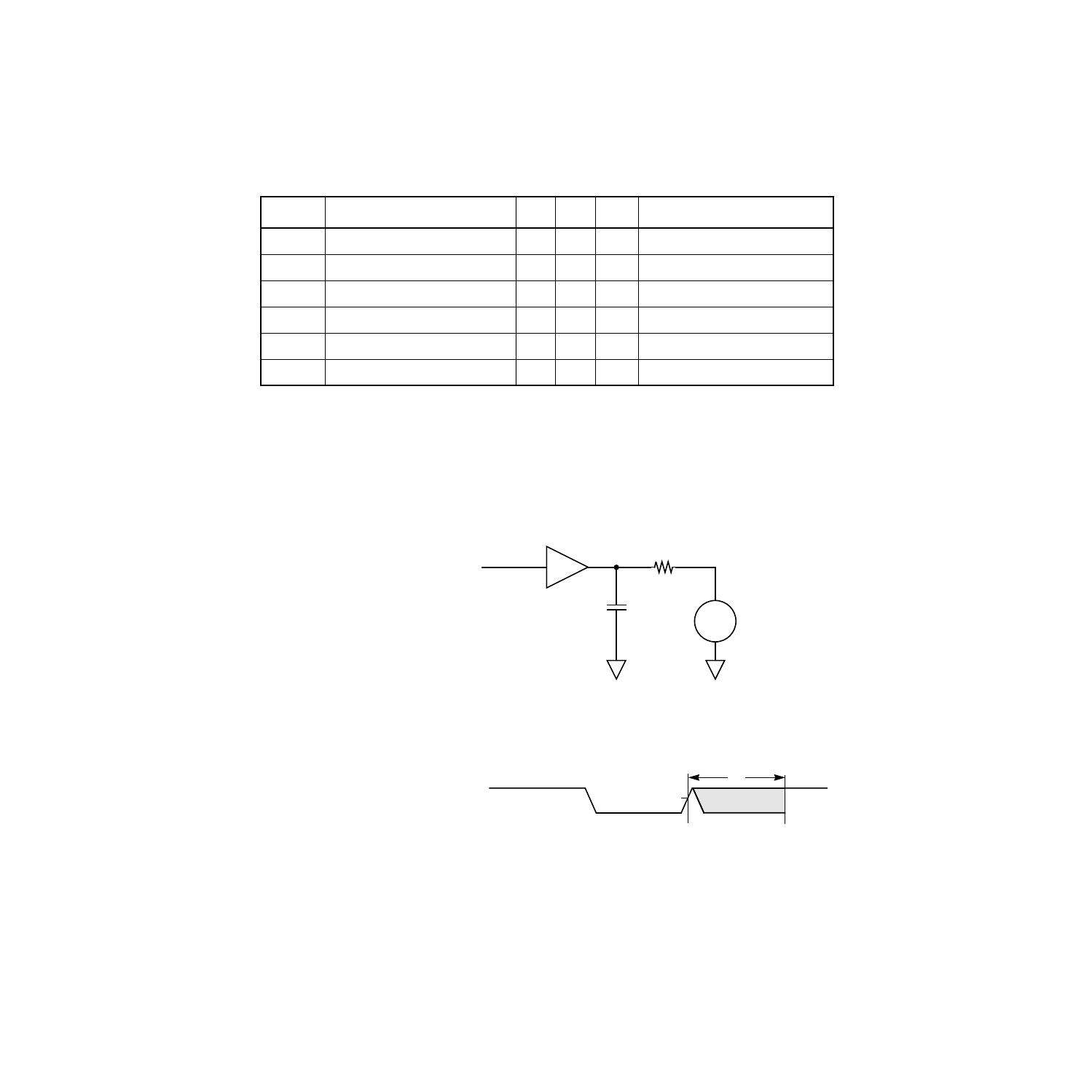
shows the SCSI input filtering described in
.
Figure 3.4
SCSI Input Filtering
shows the hysteresis of a SCSI receiver.
t
F
Fall time, 90% to 10%
5.2
14.7
ns
dV
H
/dt
Slew rate, low to high
0.15
0.49
V/ns
dV
L
/dt
Slew rate, high to low
0.19
0.67
V/ns
ESD
Electrostatic discharge
2
–
KV
MIL-STD-883C; 3015-7
Latch-up
100
–
mA
–
t
1
Filter delay
10
15
ns
1. These values are guaranteed by periodic characterization; they are not 100% tested on every device.
2. Active negation outputs only: Data, Parity, SREQ/, SACK/
3. Single pin only; irreversible damage may occur if sustained for one second.
4. SCSI RESET pin has 10 k
Ω
pull-up resistor.
Table 3.17
TolerANT Technology Electrical Characteristics
1
(Cont.)
Symbol
Parameter
Min
Max
Units
Test Conditions
20 pF
47
Ω
2.5 V
+
−
REQ/ or ACK/ Input
t
1
V
TL
Note: t
1
is the input filtering period.