Clock timing, Input timing, Output timing – Avago Technologies LSI53C120 User Manual
Page 46: Figure 3.8
Advertising
3-16
Specifications
Figure 3.8
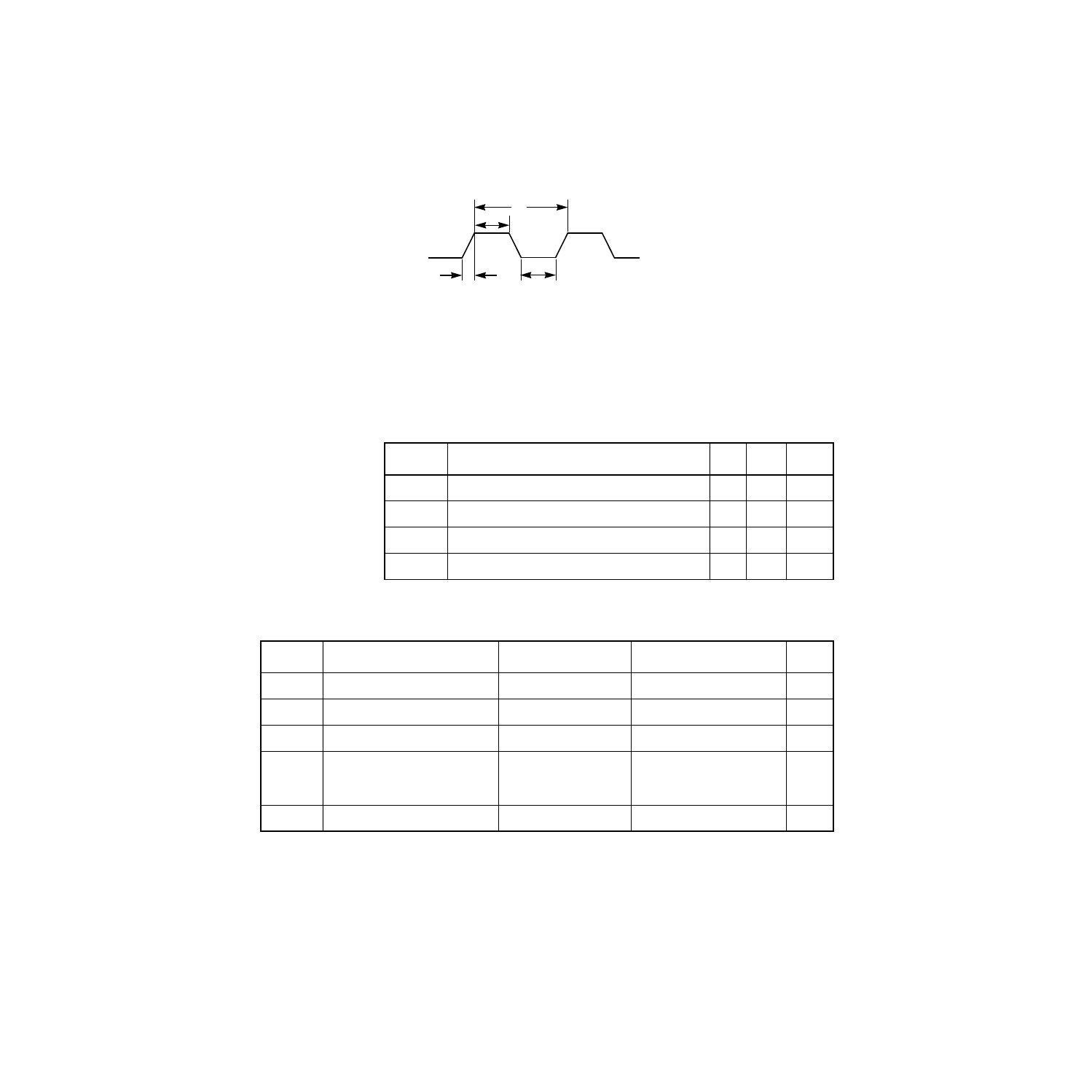
Clock Timing
3.2.3.1 SCSI Interface Timing
shows the SCSI interface input timing,
shows the
SCSI interface output timing, and
on
shows the
input/output timing diagram.
CLOCK
t
1
t
3
t
4
t
2
Table 3.19
Input Timing
Symbol
Parameter
Min
Max
Units
t
1
Input data setup
1
-
ns
t
2
Input data hold
6
-
ns
t
3
Input REQ/ACK assertion pulse width
11
-
ns
t
4
Input REQ/ACK deassertion pulse width
16
-
ns
Table 3.20
Output Timing
Symbol
Parameter
Min
Max
Units
t
5
Output data setup
min [t
1
+ 17ns, t
4
+5]
–
ns
t
6
Output data hold
max [24, (t
2
- 20), t
3
]
–
ns
t
7
Output REQ/ACK pulse width max [20 ns, t
3
-5]
max [30 ns, t
3
+5]
ns
t
8
REQ/ACK transport delay
25 ns if REQ/ACK is
clock for input data,
10 ns if not
50 ns if REQ/ACK is clock
for input data, 30 ns if not
ns
t
9
Data transport delay
6
[t
3
+35]
ns
Advertising