Specifications, Verilog hdl prototype, Vhdl component declaration – Altera SCFIFO User Manual
Page 2: Vhdl library-use declaration, Scfifo and dcfifo signals
Specifications
Verilog HDL Prototype
You can locate the Verilog HDL prototype in the Verilog Design File (.v) altera_mf.v in the <Quartus II
installation directory>\eda\synthesis directory.
VHDL Component Declaration
The VHDL component declaration is located in the
<Quartus II installation directory>\libraries\vhdl\altera_mf\
altera_mf_components.vhd
VHDL LIBRARY-USE Declaration
The VHDL LIBRARY-USE declaration is not required if you use the VHDL Component Declaration.
LIBRARY altera_mf;
USE altera_mf_altera_mf_components.all;
SCFIFO and DCFIFO Signals
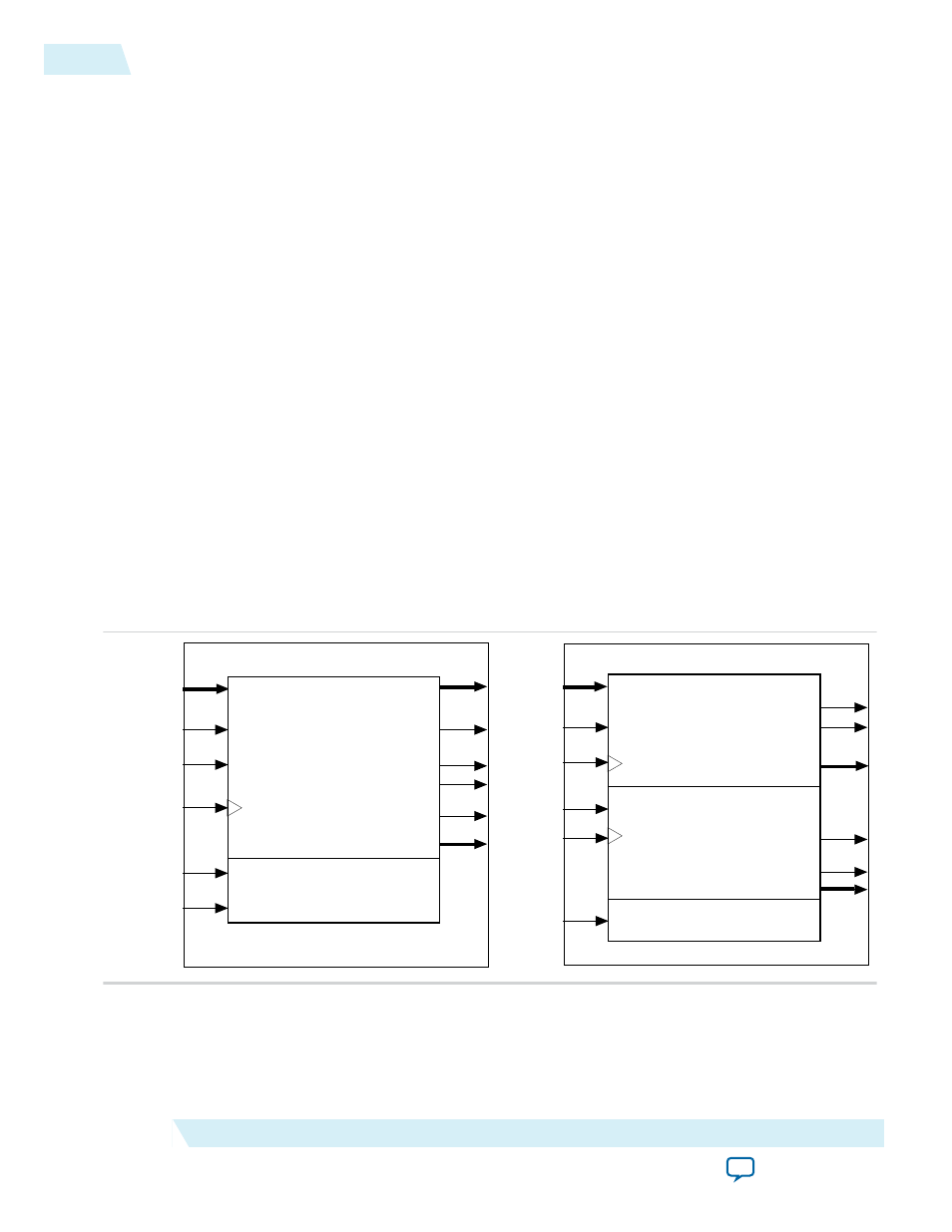
This section provides diagrams of the SCFIFO and DCFIFO blocks to help in visualizing their input and
output ports. This section also describes each port in detail to help in understanding their usages,
functionality, or any restrictions. For better illustrations, some descriptions might refer you to a specific
section in this user guide.
Figure 1: SCFIFO and DCFIFO IP Cores Input and Output Signals
SCFIFO
data[7..0]
wrreq
rdreq
sclr
aclr
clock
almost_full
almost_empty
usedw[7..0]
empty
full
q[7..0]
DCFIFO
data[7..0]
wrreq
rdreq
wrempty
aclr
rdempty
rdusedw[8..0]
wrclk
wrusedw[8..0]
q[7..0]
rdfull
wrfull
rdclk
For the SCFIFO block, the read and write signals are synchronized to the same clock; for the DCFIFO
block, the read and write signals are synchronized to the
rdclk
and
wrclk
clocks respectively. The
prefixes
wr
and
rd
represent the signals that are synchronized by the
wrclk
and
rdclk
clocks respectively.
2
Specifications
UG-MFNALT_FIFO
2014.12.17
Altera Corporation
SCFIFO and DCFIFO IP Cores User Guide