The clock control, The clock control –27 – Altera Arria V GX FPGA User Manual
Page 49
Chapter 6: Board Test System
6–27
The Clock Control
July 2012
Altera Corporation
Arria V GX FPGA Development Kit
User Guide
The Clock Control
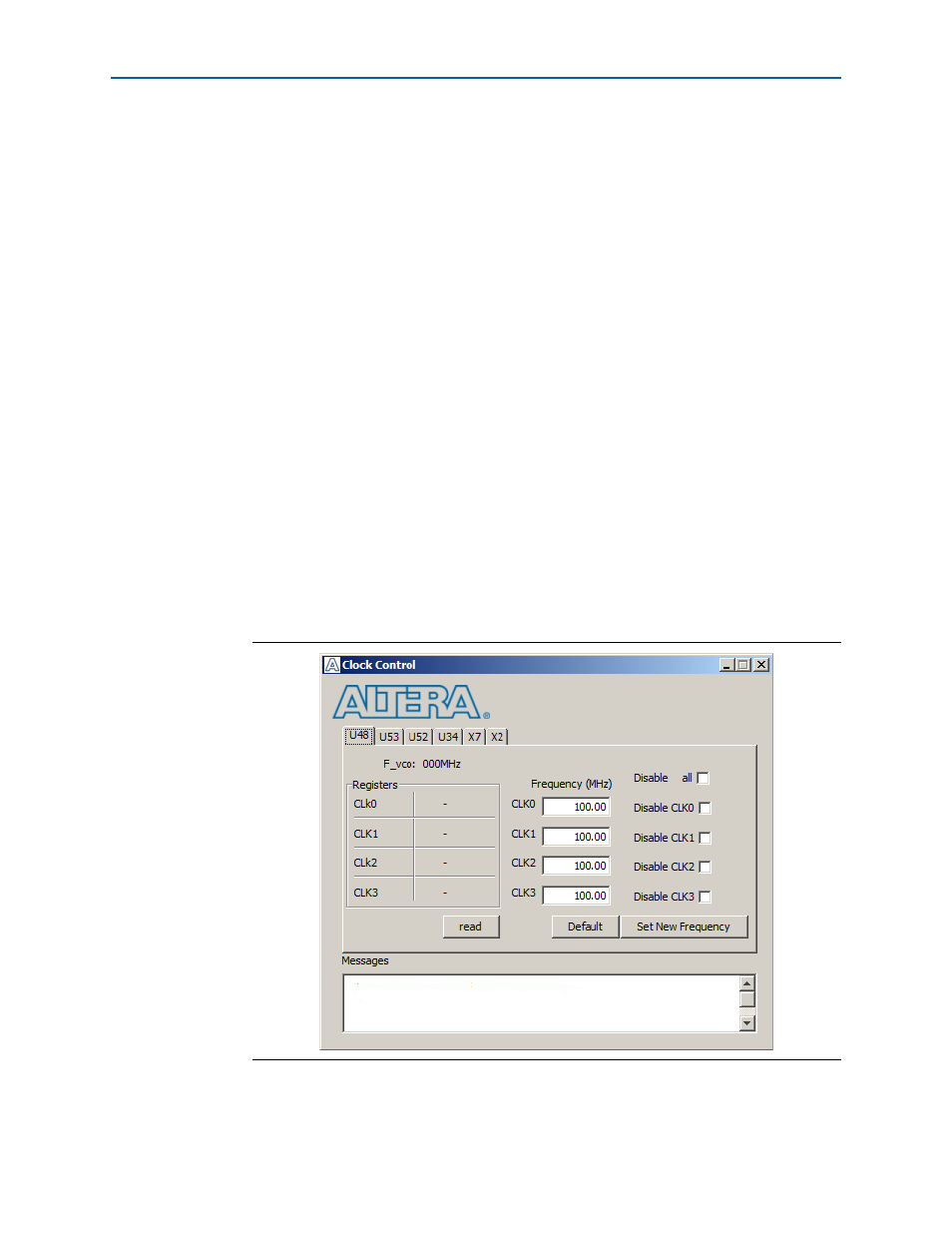
The Clock Control application sets the Si570 and Si571 programmable oscillators to
any frequency between 10 MHz and 810 MHz with eight digits of precision to the
right of the decimal point. The Si570 oscillator drives a 1-to-6 buffer that drives a copy
of the clock to the top and bottom edges of each FPGA in addition to REFCLK1 on the
left side of each FPGA. There are also four Si5338A custom devices, which output 4
programmable clocks to each FPGA. There are two of these devices dedicated to each
FPGA. Each Si5338A device provides three transceiver reference clocks to the FPGA
as well as an additional clock to one of the edges of the FPGA. In addition, Clk1 on
U53 drives a 1-to-2 clock buffer to output clocks to REFCLK3 on the left side of
FPGA 1 and to a Samtec Bullseye SMA connector (J16).
The Clock Control application runs as a stand-alone application. ClockControl.exe
resides in the <install
dir>\kits\arriaVGX_5agxfb3hf40es_fpga\examples\board_test_system directory.
On Windows, click Start > All Programs > Altera > Arria V GX FPGA Development
Kit
<version> > Clock Control to start the application.
f
For more information about the Si570, Si571, and Si5338A and the Arria V GX FPGA
development board’s clocking circuitry and clock input pins, refer to the
.
The Clock Control communicates with the MAX II device on the board through the
JTAG bus. The Si570 and Si571 (X7, X2) programmable oscillators are connected to the
MAX II device through a 2-wire serial bus.
shows the Clock Control.
The following sections describe the Clock Control controls.
Figure 6–11. The Clock Control