Altera Audio Video Development Kit, Stratix IV GX Edition User Manual
Page 30
6–8
Chapter 6: Board Test System
Using the Board Test System
Audio Video Development Kit, Stratix IV GX Edition User Guide
© November 2009 Altera
Corporation
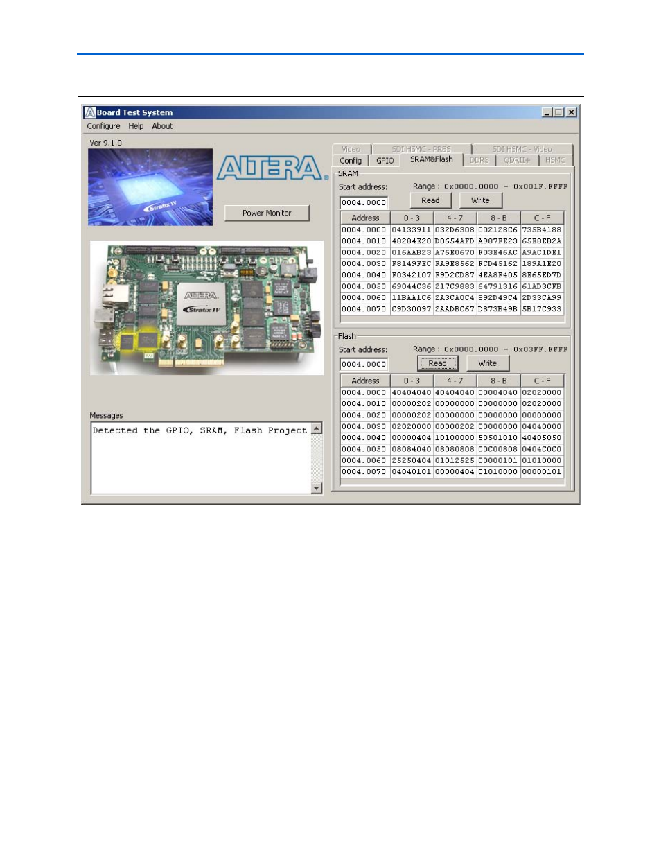
The following sections describe the controls on the SRAM&Flash tab.
SRAM
The SRAM control allows you to read and write the SRAM on your board. Type a
starting address in the text box and click Read. Values starting at the specified address
appear in the table. The SRAM addresses display in the format the Nios II processor
within the FPGA uses, that is, each SRAM address is offset by 0x00400000. Thus, the
first location in SRAM appears as 0x00400000 in the GUI.
1
If you enter an address outside of the 0x00400000 to 0x005FFFFF SRAM address
space, a warning message identifies the valid SRAM address range.
To update the SRAM contents, change values in the table and click Write. The
application writes the new values to SRAM and then reads the values back to
guarantee that the graphical display accurately reflects the memory contents.
Figure 6–4. The SRAM&Flash Tab