4 fpga register mapping, 1 lpc i/o register map, Table 6-38 – Artesyn ATCA-7365-CE Installation and Use (May 2014) User Manual
Page 185: Divisor latch lsb register (dll), if dlab=1, Table 6-39, Divisor latch msb register (dlm), if dlab=1, Maps and registers
Maps and Registers
ATCA-7365-CE Installation and Use (6806800L73J)
185
A Divisor value of 0 in the Divisor Latch Register is not allowed.
6.4
FPGA Register Mapping
6.4.1
LPC I/O Register Map
The FPGA registers may be accessed via LPC I/O cycles in the I/O address range REGISTERS. See
. For LPC register access, use the base address 0x600 and add the Address Offset. An
LPC I/O write access to an address not listed in this table or not marked with an “X” in the LPC
I/O column is ignored. A corresponding read access delivers always zero.
Note: LPC I/O Address = 0x600 + Address Offset
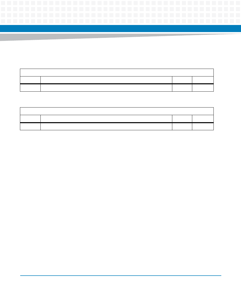
Table 6-38 Divisor Latch LSB Register (DLL), if DLAB=1
LPC IO Address: Base
Bit
Description
Default
Access
7:0
Divisor Latch LSB (DLL)
Undef.
LPC: r/w
Table 6-39 Divisor Latch MSB Register (DLM), if DLAB=1
LPC IO Address: Base + 1
Bit
Description
Default
Access
7:0
Divisor Latch MSB (DLM)
Undef.
LPC: r/w