Chapter 3 – DFI CR900-B User Manual
Page 24
www.dfi.com
Chapter 3 Hardware Installation
24
Chapter 3
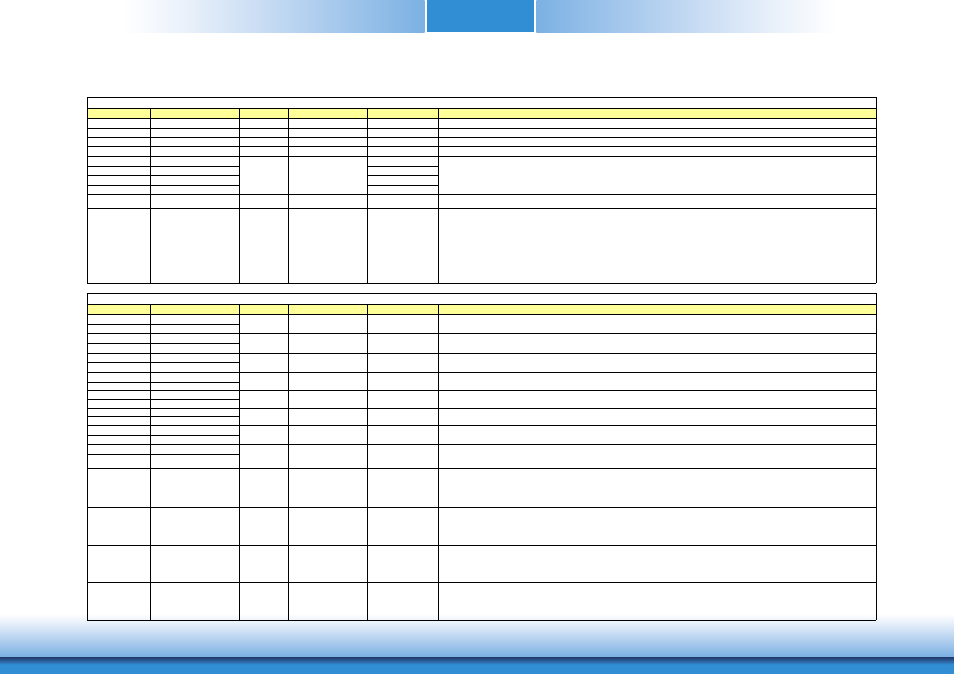
Signal
Pin#
Pin Type
Pwr Rail /Tolerance
PU/PD
Description
AC/HAD_RST#
A30
O CMOS
3.3V Suspend/3.3V
Reset output to CODEC, active low.
AC/HDA_SYNC
A29
O CMOS
3.3V/3.3V
PD 1M
Sample-synchronization signal to the CODEC(s).
AC/HDA_BITCLK A32
I/O CMOS
3.3V/3.3V
Serial data clock generated by the external CODEC(s).
AC/HDA_SDOUT A33
O CMOS
3.3V/3.3V
Serial TDM data output to the CODEC.
AC/HDA_SDIN2
B28
I/O CMOS
3.3V Suspend/3.3V
AC/HDA_SDIN1
B29
I/O CMOS
3.3V Suspend/3.3V
AC/HDA_SDIN0
B30
I/O CMOS
3.3V Suspend/3.3V
Signal
Pin#
Pin Type
Pwr Rail /Tolerance
PU/PD
Description
GBE0_MDI0+
A13
I/O Analog
3.3V max Suspend
GBE0_MDI0-
A12
I/O Analog
3.3V max Suspend
GBE0_MDI1+
A10
I/O Analog
3.3V max Suspend
GBE0_MDI1-
A9
I/O Analog
3.3V max Suspend
GBE0_MDI2+
A7
I/O Analog
3.3V max Suspend
GBE0_MDI2-
A6
I/O Analog
3.3V max Suspend
GBE0_MDI3+
A3
I/O Analog
3.3V max Suspend
GBE0_MDI3-
A2
I/O Analog
3.3V max Suspend
GBE0_ACT#
B2
OD CMOS
3.3V Suspend/3.3V
Gigabit Ethernet Controller 0 activity indicator, active low.
GBE0_LINK#
A8
OD CMOS
3.3V Suspend/3.3V
Gigabit Ethernet Controller 0 link indicator, active low.
GBE0_LINK100# A4
OD CMOS
3.3V Suspend/3.3V
Gigabit Ethernet Controller 0 100 Mbit / sec link indicator, active low.
GBE0_LINK1000# A5
OD CMOS
3.3V Suspend/3.3V
Gigabit Ethernet Controller 0 1000 Mbit / sec link indicator, active low.
GBE0_CTREF
A14
REF
GND min 3.3V max
N.C.
Reference voltage for Carrier Board Ethernet channel 0 magnetics center
tap. The reference voltage is determined by the requirements of the
Module PHY and may be as low as 0V and as high as 3.3V.
The reference voltage output shall be current limited on the Module. In
the case in which the reference
Signal
Pin#
Pin Type
Pwr Rail /Tolerance
PU/PD
Description
IDE_D0
D7
IDE_D1
C10
IDE_D2
C8
IDE_D3
C4
IDE_D4
D6
IDE_D5
D2
IDE_D6
C3
IDE_D7
C2
PD 10K to GND
IDE_D8
C6
IDE_D9
C7
IDE_D10
D3
IDE_D11
D4
IDE_D12
D5
IDE_D13
C9
IDE_D14
C12
IDE_D15
C5
IDE_A0
D13
IDE_A1
D14
IDE_A2
D15
IDE_IOW#
D9
O CMOS
3.3V / 3.3V
I/O write line to IDE device. Data latched on trailing (rising) edge.
IDE_IOR#
C14
O CMOS
3.3V / 3.3V
I/O read line to IDE device.
IDE_REQ
D8
I CMOS
3.3V / 5V
PD 5.6K to GND
IDE Device DMA Request. It is asserted by the IDE device to request a data transfer.
IDE_ACK#
D10
O CMOS
3.3V / 3.3V
IDE Device DMA Acknowledge.
IDE_CS1#
D16
O CMOS
3.3V / 3.3V
IDE Device Chip Select for 1F0h to 1FFh range.
IDE_CS3#
D17
O CMOS
3.3V / 3.3V
IDE Device Chip Select for 3F0h to 3FFh range.
IDE_IORDY
C13
I CMOS
3.3V / 5V
PU 4.7K to 3.3V
IDE device I/O ready input. Pulled low by the IDE device to extend the cycle.
IDE_RESET#
D18
O CMOS
3.3V / 3.3V
Reset output to IDE device, active low.
IDE_IRQ
D12
I CMOS
3.3V / 5V
PD 10K to GND
Interrupt request from IDE device.
IDE_CBLID#
D77
I CMOS
3.3V / 5V
Input from off-Module hardware indicating the type of IDE cable being
used. High indicates a 40-pin cable used for legacy IDE modes. Low
indicates that an 80-pin cable with interleaved grounds is used. Such a
cable is required for Ultra-DMA 66, 100 and 133 modes.
Signal
Pin#
Pin Type
Pwr Rail /Tolerance
PU/PD
Description
SATA0_TX+
A16
O SATA
AC coupled on Module
SATA0_TX-
A17
O SATA
AC coupled on Module
SATA0_RX+
A19
I SATA
AC coupled on Module
SATA0_RX-
A20
I SATA
AC coupled on Module
SATA1_TX+
B16
O SATA
AC coupled on Module
SATA1_TX-
B17
O SATA
AC coupled on Module
SATA1_RX+
B19
I SATA
AC coupled on Module
SATA1_RX-
B20
I SATA
AC coupled on Module
SATA2_TX+
A22
O SATA
AC coupled on Module
SATA2_TX-
A23
O SATA
AC coupled on Module
SATA2_RX+
A25
I SATA
AC coupled on Module
SATA2_RX-
A26
I SATA
AC coupled on Module
SATA3_TX+
B22
O SATA
AC coupled on Module
SATA3_TX-
B23
O SATA
AC coupled on Module
SATA3_RX+
B25
I SATA
AC coupled on Module
SATA3_RX-
B26
I SATA
AC coupled on Module
ATA_ACT#
A28
I/O CMOS
3.3V / 3.3V
PU 10K to 3.3V
ATA (parallel and serial) or SAS activity indicator, active low.
Signal
Pin#
Pin Type
Pwr Rail /Tolerance
PU/PD
Description
PCIE_TX0+
A68
PCIE_TX0-
A69
PCIE_RX0+
B68
PCIE_RX0-
B69
PCIE_TX1+
A64
PCIE_TX1-
A65
PCIE_RX1+
B64
PCIE_RX1-
B65
PCIE_TX2+
A61
PCIE_TX2-
A62
PCIE_RX2+
B61
PCIE_RX2-
B62
PCIE_TX3+
A58
PCIE_TX3-
A59
PCIE_RX3+
B58
PCIE_RX3-
B59
PCIE_TX4+
A55
PCIE_TX4-
A56
PCIE_RX4+
B55
PCIE_RX4-
B56
PCIE_TX5+
A52
PCIE_TX5-
A53
PCIE_RX5+
B52
PCIE_RX5-
B53
PCIE0_CK_REF+ A88
PCIE0_CK_REF-
A89
Signal
Pin#
Pin Type
Pwr Rail /Tolerance
PU/PD
Description
PEG_TX0+
D52
PEG_TX0-
D53
PEG_RX0+
C52
PEG_RX0-
C53
PEG_TX1+
D55
PEG_TX1-
D56
PEG_RX1+
C55
PEG_RX1-
C56
PEG_TX2+
D58
PEG_TX2-
D59
PEG_RX2+
C58
PEG_RX2-
C59
PEG_TX3+
D61
PEG_TX3-
D62
PEG_RX3+
C61
PEG_RX3-
C62
PEG_TX4+
D65
PEG_TX4-
D66
PEG_RX4+
C65
PEG_RX4-
C66
PEG_TX5+
D68
PEG_TX5-
D69
PEG_RX5+
C68
PEG_RX5-
C69
PEG_TX6+
D71
PEG_TX6-
D72
PEG_RX6+
C71
PEG_RX6-
C72
PEG_TX7+
D74
PEG_TX7-
D75
PEG_RX7+
C74
PEG_RX7-
C75
PEG_TX8+
D78
PEG_TX8-
D79
PEG_RX8+
C78
PEG_RX8-
C79
PEG_TX9+
D81
PEG_TX9-
D82
PEG_RX9+
C81
PEG_RX9-
C82
PEG_TX10+
D85
PEG_TX10-
D86
PEG_RX10+
C85
PEG_RX10-
C86
PEG_TX11+
D88
PEG_TX11-
D89
PEG_RX11+
C88
PEG_RX11-
C89
PEG_TX12+
D91
PEG_TX12-
D92
PEG_RX12+
C91
PEG_RX12-
C92
PEG_TX13+
D94
PEG_TX13-
D95
PEG_RX13+
C94
PEG_RX13-
C95
PEG_TX14+
D98
PEG_TX14-
D99
PEG_RX14+
C98
PEG_RX14-
C99
PEG_TX15+
D101
PEG_TX15-
D102
PEG_RX15+
C101
PEG_RX15-
C102
PEG_LANE_RV#
D54
I CMOS
3.3V / 3.3V
PU 10K to 1.05V
PCI Express Graphics lane reversal input strap. Pull low on the Carrier
board to reverse lane order.
PEG_ENABLE#
D97
I CMOS
3.3V /3.3V
PU 10K to 3.3V
Strap to enable PCI Express x16 external graphics interface. Pull low to
enable the x16 PEG interface.
Signal
Pin#
Pin Type
Pwr Rail /Tolerance
PU/PD
Description
EXCD0_CPPE#
A49
EXCD1_CPPE#
B48
EXCD0_PERST#
A48
EXCD1_PERST#
B47
Signal
Pin#
Pin Type
Pwr Rail /Tolerance
PU/PD
Description
PCI_AD0
C24
PCI_AD1
D22
PCI_AD2
C25
PCI_AD3
D23
PCI_AD4
C26
PCI_AD5
D24
PCI_AD6
C27
PCI_AD7
D25
PCI_AD8
C28
PCI_AD9
D27
PCI_AD10
C29
PCI_AD11
D28
PCI_AD12
C30
PCI_AD13
D29
PCI_AD14
C32
PCI_AD15
D30
PCI_AD16
D37
PCI_AD17
C39
PCI_AD18
D38
PCI_AD19
C40
PCI_AD20
D39
PCI_AD21
C42
PCI_AD22
D40
PCI_AD23
C43
PCI_AD24
D42
PCI_AD25
C45
PCI_AD26
D43
PCI_AD27
C46
PCI_AD28
D44
PCI_AD29
C47
PCI_AD30
D45
PCI_AD31
C48
PCI_C/BE0#
D26
PCI_C/BE1#
C33
PCI_C/BE2#
C38
PCI_C/BE3#
C44
PCI_DEVSEL#
C36
I/O CMOS
3.3V / 5V
PU 8.2K to 3.3V
PCI bus Device Select, active low.
PCI_FRAME#
D36
I/O CMOS
3.3V / 5V
PU 8.2K to 3.3V
PCI bus Frame control line, active low.
PCI_IRDY#
C37
I/O CMOS
3.3V / 5V
PU 8.2K to 3.3V
PCI bus Initiator Ready control line, active low.
PCI_TRDY#
D35
I/O CMOS
3.3V / 5V
PU 8.2K to 3.3V
PCI bus Target Ready control line, active low.
PCI_STOP#
D34
I/O CMOS
3.3V / 5V
PU 8.2K to 3.3V
PCI bus STOP control line, active low, driven by cycle initiator.
PCI_PAR
D32
I/O CMOS
3.3V / 5V
PCI bus parity
PCI_PERR#
C34
I/O CMOS
3.3V / 5V
PU 8.2K to 3.3V
Parity Error: An external PCI device drives PERR# when it receives data that has a parity error.
PCI_REQ0#
C22
PU 8.2K to 3.3V
PCI_REQ1#
C19
PU 8.2K to 3.3V
PCI_REQ2#
C17
PU 8.2K to 3.3V
PCI_REQ3#
D20
PU 8.2K to 3.3V
PCI_GNT0#
C20
PCI_GNT1#
C18
PCI_GNT2#
C16
PCI_GNT3#
D19
PCI_RESET#
C23
O CMOS
3.3V Suspend/ 5V
PCI Reset output, active low.
PCI_LOCK#
C35
I/O CMOS
3.3V / 5V
PU 8.2K to 3.3V
PCI Lock control line, active low.
PCI_SERR#
D33
I/O OD CMOS 3.3V / 5V
PU 8.2K to 3.3V
System Error: SERR# may be pulsed active by any PCI device that detects a system error condition.
PCI_PME#
C15
I CMOS
3.3V Suspend/ 5V
PU 10K to 3.3VSB PCI Power Management Event: PCI peripherals drive PME# to wake system from low-power states S1–S5.
PCI_CLKRUN#
D48
I/O CMOS
3.3V / 5V
PU 8.2K to 3.3V
Bidirectional pin used to support PCI clock run protocol for mobile systems.
PCI_IRQA#
C49
PU 8.2K to 3.3V
PCI_IRQB#
C50
PU 8.2K to 3.3V
PCI_IRQC#
D46
PU 8.2K to 3.3V
PCI_IRQD#
D47
PU 8.2K to 3.3V
PCI_CLK
D50
O CMOS
3.3V / 3.3V
PCI 33MHz clock output.
PCI_M66EN
D49
I CMOS
3.3V / 5V
PD 10K to GND
Module input signal indicates whether an off-Module PCI device is
capable of 66MHz operation. Pulled to GND by Carrier Board device or
by Slot Card if the devices are NOT capable of 66 MHz operation.
If the Module is not capable of supporting 66 MHz PCI operation, this
input may be a no-connect on the Module.
If the Module is capable of supporting 66 MHz PCI operation, and if this
input is held low by the Carrier Board, the Module PCI interface shall
operate at 33 MHz.
Signal
Pin#
Pin Type
Pwr Rail /Tolerance
PU/PD
Description
USB0+
A46
USB0-
A45
USB1+
B46
USB1-
B45
USB2+
A43
USB2-
A42
USB3+
B43
USB3-
B42
USB4+
A40
USB4-
A39
USB5+
B40
USB5-
B39
USB6+
A37
USB6-
A36
USB7+
B37
USB7-
B36
USB_0_1_OC#
B44
I CMOS
3.3V Suspend/3.3V
PU 10K to 3.3VSB
USB over-current sense, USB channels 0 and 1. A pull-up for this line
shall be present on the Module. An open drain driver from a USB
current monitor on the Carrier Board may drive this line low. Do not
pull this line high on the Carrier Board.
USB_2_3_OC#
A44
I CMOS
3.3V Suspend/3.3V
PU 10K to 3.3VSB
USB over-current sense, USB channels 2 and 3. A pull-up for this line
shall be present on the Module. An open drain driver from a USB
current monitor on the Carrier Board may drive this line low. Do not
pull this line high on the Carrier Board.
USB_4_5_OC#
B38
I CMOS
3.3V Suspend/3.3V
PU 10K to 3.3VSB
USB over-current sense, USB channels 4 and 5. A pull-up for this line
shall be present on the Module. An open drain driver from a USB
current monitor on the Carrier Board may drive this line low. Do not
pull this line high on the Carrier Board.
USB_6_7_OC#
A38
I CMOS
3.3V Suspend/3.3V
PU 10K to 3.3VSB
USB over-current sense, USB channels 6 and 7. A pull-up for this line
shall be present on the Module. An open drain driver from a USB
current monitor on the Carrier Board may drive this line low. Do not
pull this line high on the Carrier Board.
Signal
Pin#
Pin Type
Pwr Rail /Tolerance
PU/PD
Description
LVDS_A0+
A71
LVDS_A0-
A72
LVDS_A1+
A73
LVDS_A1-
A74
LVDS_A2+
A75
LVDS_A2-
A76
LVDS_A3+
A78
LVDS_A3-
A79
LVDS_A_CK+
A81
LVDS_A_CK-
A82
LVDS_B0+
B71
LVDS_B0-
B72
LVDS_B1+
B73
LVDS_B1-
B74
LVDS_B2+
B75
LVDS_B2-
B76
LVDS_B3+
B77
LVDS_B3-
B78
LVDS_B_CK+
B81
LVDS_B_CK-
B82
LVDS_VDD_EN
A77
O CMOS
3.3V / 3.3V
PD 100K to GND
LVDS panel power enable
LVDS_BKLT_EN
B79
O CMOS
3.3V / 3.3V
PD 100K to GND
LVDS panel backlight enable
LVDS_BKLT_CTRL B83
O CMOS
3.3V / 3.3V
PD 100K to GND
LVDS panel backlight brightness control
LVDS_I2C_CK
A83
I/O OD CMOS 3.3V / 3.3V
PU 2.2K to 3.3V
I2C clock output for LVDS display use
LVDS_I2C_DAT
A84
I/O OD CMOS 3.3V / 3.3V
PU 2.2K to 3.3V
I2C data line for LVDS display use
Signal
Pin#
Pin Type
Pwr Rail /Tolerance
PU/PD
Description
LPC_AD0
B4
LPC_AD1
B5
LPC_AD2
B6
LPC_AD3
B7
LPC_FRAME#
B3
O CMOS
3.3V / 3.3V
LPC frame indicates the start of an LPC cycle
LPC_DRQ0#
B8
LPC_DRQ1#
B9
LPC_SERIRQ
A50
I/O CMOS
3.3V / 3.3V
PU 10K to 3.3V
LPC serial interrupt
LPC_CLK
B10
O CMOS
3.3V / 3.3V
LPC clock output - 33MHz nominal
Signal
Pin#
Pin Type
Pwr Rail /Tolerance
PU/PD
Description
SPI_CS#
B97
O CMOS
3.3V Suspend/3.3V
Chip select for Carrier Board SPI - may be sourced from chipset SPI0 or SPI1
SPI_MISO
A92
I CMOS
3.3V Suspend/3.3V
Data in to Module from Carrier SPI
SPI_MOSI
A95
O CMOS
3.3V Suspend/3.3V
Data out from Module to Carrier SPI
SPI_CLK
A94
O CMOS
3.3V Suspend/3.3V
Clock from Module to Carrier SPI
SPI_POWER
A91
O
3.3V Suspend/3.3V
Power supply for Carrier Board SPI – sourced from Module – nominally
3.3V. The Module shall provide a minimum of 100mA on SPI_POWER.
Carriers shall use less than 100mA of SPI_POWER. SPI_POWER
shall only be used to power SPI devices on the Carrier
BIOS_DIS0#
A34
BIOS_DIS1#
B88
Signal
Pin#
Pin Type
Pwr Rail /Tolerance
PU/PD
Description
VGA_RED
B89
O Analog
Analog
PD 150
Red for monitor. Analog output
VGA_GRN
B91
O Analog
Analog
PD 150
Green for monitor. Analog output
VGA_BLU
B92
O Analog
Analog
PD 150
Blue for monitor. Analog output
VGA_HSYNC
B93
O CMOS
3.3V / 3.3V
Horizontal sync output to VGA monitor
VGA_VSYNC
B94
O CMOS
3.3V / 3.3V
Vertical sync output to VGA monitor
VGA_I2C_CK
B95
I/O OD CMOS 3.3V / 3.3V
PU 2.2K to 3.3V
DDC clock line (I2C port dedicated to identify VGA monitor capabilities)
VGA_I2C_DAT
B96
I/O OD CMOS 3.3V / 3.3V
PU 2.2K to 3.3V
DDC data line.
Signal
Pin#
Pin Type
Pwr Rail /Tolerance
PU/PD
Description
I2C_CK
B33
I/O OD CMOS 3.3V Suspend/3.3V
PU 2.2K to 3.3VSB General purpose I2C port clock output
I2C_DAT
B34
I/O OD CMOS 3.3V Suspend/3.3V
PU 2.2K to 3.3VSB General purpose I2C port data I/O line
Signal
Pin#
Pin Type
Pwr Rail /Tolerance
PU/PD
Description
SPKR
B32
O CMOS
3.3V / 3.3V
Output for audio enunciator - the "speaker" in PC-AT systems.
This port provides the PC beep signal and is mostly intended for
debugging purposes.
WDT
B27
O CMOS
3.3V / 3.3V
Output indicating that a watchdog time-out event has occurred.
KBD_RST#
A86
I CMOS
3.3V / 3.3V
PU 10K to 3.3V
Input to Module from (optional) external keyboard controller that can force a reset. Pulled high on the Module. This is a legacy
artifact of the PC-AT.
KBD_A20GATE
A87
I CMOS
3.3V / 3.3V
PU 10K to 3.3V
Input to Module from (optional) external keyboard controller that can be used to control the CPU A20 gate line. The A20GATE
restricts the memory access to the bottom megabyte and is a legacy artifact of the PC-AT.Pulled high on the Module.
Signal
Pin#
Pin Type
Pwr Rail /Tolerance
PU/PD
Description
PWRBTN#
B12
I CMOS
3.3V Suspend/3.3V
PU 10K to 3.3VSB
A falling edge creates a power button event. Power button events can
be used to bring a system out of S5 soft off and other suspend states,
as well as powering the system down.
SYS_RESET#
B49
I CMOS
3.3V Suspend/3.3V
PU 10K to 3.3VSB
Reset button input. Active low request for Module to reset and reboot.
May be falling edge sensitive. For situations when SYS_RESET# is
not able to reestablish control of the system, PWR_OK or a power
cycle may be used.
CB_RESET#
B50
O CMOS
3.3V Suspend/3.3V
PD 100K to GND
Reset output from Module to Carrier Board. Active low. Issued by
Module chipset and may result from a low SYS_RESET# input, a low
PWR_OK input, a VCC_12V power input that falls below the minimum
specification, a watchdog timeout, or may be initiated by the Module
software.
PWR_OK
B24
I CMOS
3.3V / 3.3V
Power OK from main power supply. A high value indicates that the
power is good. This signal can be used to hold off Module startup to
allow Carrier based FPGAs or other configurable devices time to be
programmed.
SUS_STAT#
B18
O CMOS
3.3V Suspend/3.3V
Indicates imminent suspend operation; used to notify LPC devices.
SUS_S3#
A15
O CMOS
3.3V Suspend/3.3V
Indicates system is in Suspend to RAM state. Active low output. An
inverted copy of SUS_S3# on the Carrier Board may be used to
enable the non-standby power on a typical ATX supply.
SUS_S4#
A18
O CMOS
3.3V Suspend/3.3V
Indicates system is in Suspend to Disk state. Active low output.
SUS_S5#
A24
O CMOS
3.3V Suspend/3.3V
Indicates system is in Soft Off state.
WAKE0#
B66
I CMOS
3.3V Suspend/3.3V
PU 10K to 3.3VSB PCI Express wake up signal.
WAKE1#
B67
I CMOS
3.3V Suspend/3.3V
PU 10K to 3.3VSB General purpose wake up signal. May be used to implement wake-up
on PS2 keyboard or mouse activity.
BATLOW#
A27
I CMOS
3.3V Suspend/ 3.3V
PU 10K to 3.3VSB
Indicates that external battery is low.
This port provides a battery-low signal to the Module for orderly
transitioning to power saving or power cut-off ACPI modes.
Signal
Pin#
Pin Type
Pwr Rail /Tolerance
PU/PD
Description
THRM#
B35
I CMOS
3.3V / 3.3V
PU 10K to 3.3V
Input from off-Module temp sensor indicating an over-temp situation.
THRMTRIP#
A35
O CMOS
3.3V / 3.3V
PU 10K to 3.3V
Active low output indicating that the CPU has entered thermal shutdown.
Signal
Pin#
Pin Type
Pwr Rail /Tolerance
PU/PD
Description
SMB_CK
B13
I/O OD CMOS 3.3V Suspend/3.3V
PU 2.2K to 3.3VSB System Management Bus bidirectional clock line.
SMB_DAT
B14
I/O OD CMOS 3.3V Suspend/3.3V
PU 2.2K to 3.3VSB System Management Bus bidirectional data line.
SMB_ALERT#
B15
I CMOS
3.3V Suspend/3.3V
PU 10K to 3.3VSB
System Management Bus Alert – active low input can be used to
generate an SMI# (System Management Interrupt) or to wake the system.
Signal
Pin#
Pin Type
Pwr Rail /Tolerance
PU/PD
Description
GPO0
A93
GPO1
B54
GPO2
B57
GPO3
B63
GPI0
A54
GPI1
A63
GPI2
A67
GPI3
A85
Signal
Pin#
Pin Type
Pwr Rail /Tolerance
PU/PD
Description
VCC_12V
A104~A109
B104~B109
C104~C109
D104~D109
Power
Primary power input: +12V nominal. All available VCC_12V pins on the connector(s) shall be used.
VCC_5V_SBY
B84~B87
Power
Standby power input: +5.0V nominal. If VCC5_SBY is used, all
available VCC_5V_SBY pins on the connector(s) shall be used. Only
used for standby and suspend functions. May be left unconnected if
these functions are not used in the system design.
VCC_RTC
A47
Power
Real-time clock circuit-power input. Nominally +3.0V.
GND
A1, A11, A21, A31, A41,
A51, A57, A60, A66, A70,
A80, A90, A96,A100,
A110, B1, B11, B21 ,B31,
B41, B51, B60, B70, B80,
B90, B100, B110, C1,C11,
C21, C31, C41, C51, C60,
C70, C76, C80, C84, C87,
C90, C93, C96, C100,
C103, C110, D1,D11,D21,
D31, D41, D51, D60,
D67, D70,D76, D80, D84,
D87, D90, D93, D96,
D100 D103 D110
Power
Ground - DC power and signal and AC signal return path.
All available GND connector pins shall be used and tied to Carrier
Board GND plane.
Signal
Pin#
Pin Type
Pwr Rail /Tolerance
PU/PD
Description
TYPE0#
C54
PDS
TYPE1#
C57
PDS
TYPE2#
D57
PDS
TYPE10#
A97
PDS
TYPE 10#
NC pin out R2.0
PD pin out Type 10 pull down to ground with 47K resistor
12V pin out R1.0
A carrier can detect a R1.0 Module by the presence of 12V on this pin. R2.0 Module types 1-6 will no connet this pin. Type 10
Modules shall pull this pin to ground through a 4.7K resistor.
Pin Types
I Input to the Module
O Output from the Module
I/O Bi-directional input / output signal
OD Open drain output
IDE Signals Descriptions
I/O CMOS
3.3V / 5V
Bidirectional data to / from IDE device.
O CMOS
3.3V / 3.3V
Address lines to IDE device.
AC97/HDA Signals Descriptions
Serial TDM data inputs from up to 3 CODECs.
Gigabit Ethernet Signals Descriptions
Gigabit Ethernet Controller 0: Media Dependent Interface Differential
Pairs 0,1,2,3. The MDI can operate in 1000, 100 and 10 Mbit / sec
modes. Some pairs are unused in some modes, per the following:
1000BASE-T 100BASE-TX 10BASE-T
MDI[0]+/- B1_DA+/- TX+/- TX+/-
MDI[1]+/- B1_DB+/- RX+/- RX+/-
MDI[2]+/- B1_DC+/-
MDI[3]+/- B1_DD+/-
Serial ATA or SAS Channel 1 receive differential pair.
Serial ATA or SAS Channel 2 transmit differential pair.
Serial ATA or SAS Channel 2 receive differential pair.
SATA Signals Descriptions
Serial ATA or SAS Channel 0 transmit differential pair.
Serial ATA or SAS Channel 0 receive differential pair.
Serial ATA or SAS Channel 1 transmit differential pair.
Serial ATA or SAS Channel 3 transmit differential pair.
Serial ATA or SAS Channel 3 receive differential pair.
PCI Express Lanes Signals Descriptions
O PCIE
AC coupled on Module
PCI Express Differential Transmit Pairs 0
I PCIE
AC coupled off Module
PCI Express Differential Receive Pairs 1
O PCIE
AC coupled on Module
PCI Express Differential Transmit Pairs 2
I PCIE
AC coupled off Module
PCI Express Differential Receive Pairs 0
O PCIE
AC coupled on Module
PCI Express Differential Transmit Pairs 1
I PCIE
AC coupled off Module
PCI Express Differential Receive Pairs 3
O PCIE
AC coupled on Module
PCI Express Differential Transmit Pairs 4
I PCIE
AC coupled off Module
PCI Express Differential Receive Pairs 2
O PCIE
AC coupled on Module
PCI Express Differential Transmit Pairs 3
I PCIE
AC coupled off Module
PCI Express Differential Receive Pairs 5
O PCIE
PCIE
Reference clock output for all PCI Express and PCI Express Graphics lanes.
I PCIE
AC coupled off Module
PCI Express Differential Receive Pairs 4
O PCIE
AC coupled on Module
PCI Express Differential Transmit Pairs 5
O PCIE
AC coupled on Module
PCI Express Graphics transmit differential pairs 1
I PCIE
AC coupled off Module
PCI Express Graphics receive differential pairs 1
PEG Signals Descriptions
O PCIE
AC coupled on Module
PCI Express Graphics transmit differential pairs 0
I PCIE
AC coupled off Module
PCI Express Graphics receive differential pairs 0
O PCIE
AC coupled on Module
PCI Express Graphics transmit differential pairs 3
I PCIE
AC coupled off Module
PCI Express Graphics receive differential pairs 3
O PCIE
AC coupled on Module
PCI Express Graphics transmit differential pairs 2
I PCIE
AC coupled off Module
PCI Express Graphics receive differential pairs 2
O PCIE
AC coupled on Module
PCI Express Graphics transmit differential pairs 5
I PCIE
AC coupled off Module
PCI Express Graphics receive differential pairs 5
O PCIE
AC coupled on Module
PCI Express Graphics transmit differential pairs 4
I PCIE
AC coupled off Module
PCI Express Graphics receive differential pairs 4
O PCIE
AC coupled on Module
PCI Express Graphics transmit differential pairs 7
I PCIE
AC coupled off Module
PCI Express Graphics receive differential pairs 7
O PCIE
AC coupled on Module
PCI Express Graphics transmit differential pairs 6
I PCIE
AC coupled off Module
PCI Express Graphics receive differential pairs 6
O PCIE
AC coupled on Module
PCI Express Graphics transmit differential pairs 9
I PCIE
AC coupled off Module
PCI Express Graphics receive differential pairs 9
O PCIE
AC coupled on Module
PCI Express Graphics transmit differential pairs 8
I PCIE
AC coupled off Module
PCI Express Graphics receive differential pairs 8
O PCIE
AC coupled on Module
PCI Express Graphics transmit differential pairs 11
I PCIE
AC coupled off Module
PCI Express Graphics receive differential pairs 11
O PCIE
AC coupled on Module
PCI Express Graphics transmit differential pairs 10
I PCIE
AC coupled off Module
PCI Express Graphics receive differential pairs 10
O PCIE
AC coupled on Module
PCI Express Graphics transmit differential pairs 13
I PCIE
AC coupled off Module
PCI Express Graphics receive differential pairs 13
O PCIE
AC coupled on Module
PCI Express Graphics transmit differential pairs 12
I PCIE
AC coupled off Module
PCI Express Graphics receive differential pairs 12
O PCIE
AC coupled on Module
PCI Express Graphics transmit differential pairs 15
I PCIE
AC coupled off Module
PCI Express Graphics receive differential pairs 15
O PCIE
AC coupled on Module
PCI Express Graphics transmit differential pairs 14
I PCIE
AC coupled off Module
PCI Express Graphics receive differential pairs 14
ExpressCard Signals Descriptions
I CMOS
3.3V /3.3V
PU 10K to 3.3V
PCI ExpressCard: PCI Express capable card request, active low, one per card
O CMOS
3.3V /3.3V
PCI ExpressCard: reset, active low, one per card
I CMOS
3.3V / 5V
PCI bus master request input lines, active low.
O CMOS
3.3V / 5V
PCI bus master grant output lines, active low.
PCI Signals Descriptions
I/O CMOS
3.3V / 5V
PCI bus multiplexed address and data lines
I/O CMOS
3.3V / 5V
PCI bus byte enable lines, active low
I/O USB
3.3V Suspend/3.3V
USB differential pairs 1
I/O USB
3.3V Suspend/3.3V
USB differential pairs 2
I CMOS
3.3V / 5V
PCI interrupt request lines.
USB Signals Descriptions
I/O USB
3.3V Suspend/3.3V
USB differential pairs 0
I/O USB
3.3V Suspend/3.3V
USB differential pairs 5
I/O USB
3.3V Suspend/3.3V
USB differential pairs 6
I/O USB
3.3V Suspend/3.3V
USB differential pairs 3
I/O USB
3.3V Suspend/3.3V
USB differential pairs 4
LVDS Channel B differential clock
LPC Signals Descriptions
I/O USB
3.3V Suspend/3.3V
USB differential pairs 7, USB7 may be configured as a USB client or as a host, or both, at the
Module designer's discretion.(CR900-B default set as a host)
LVDS Signals Descriptions
O LVDS
LVDS
LVDS Channel A differential pairs
O LVDS
LVDS
O LVDS
LVDS
O LVDS
LVDS
I/O CMOS
3.3V / 3.3V
LPC multiplexed address, command and data bus
LVDS Channel A differential clock
O LVDS
LVDS
LVDS Channel B differential pairs
O LVDS
LVDS
O LVDS
LVDS
O LVDS
LVDS
O LVDS
LVDS
O LVDS
LVDS
I CMOS
3.3V / 3.3V
LPC serial DMA request
SPI Signals Descriptions
I CMOS
NA
Selection straps to determine the BIOS boot device.
The Carrier should only float these or pull them low, please refer to
COM Express Module Base Specification Revision 2.1 for strapping options of BIOS disable signals.
Module type Signal Descriptions
TYPE2# TYPE1# TYPE0#
X X X pin out Type 1
NC NC NC pin out Type 2
NC NC GND pin out Type 3 (no IDE)
NC GND NC pin out Type 4 (no PCI)
NC GND GND pin out Type 5 (no IDE, no PCI)
GND NC NC pin out Type 6 (no IDE, no PCI)
I CMOS
3.3V Suspend / 3.3V
General purpose input pins.
Power and GND Signal Descriptions
VGA Signals Descriptions
I2C BUS Signal Descriptions
Power and System Management Signals Descriptions
GPIO Signals Descriptions
O CMOS
3.3V / 3.3V
General purpose output pins.
Miscellaneous Signal Descriptions
Thermal Protectiont Signals Descriptions
SM Bus Signals Descriptions
Signal
Pin#
Pin Type
Pwr Rail /Tolerance
PU/PD
Description
AC/HAD_RST#
A30
O CMOS
3.3V Suspend/3.3V
Reset output to CODEC, active low.
AC/HDA_SYNC
A29
O CMOS
3.3V/3.3V
PD 1M
Sample-synchronization signal to the CODEC(s).
AC/HDA_BITCLK A32
I/O CMOS
3.3V/3.3V
Serial data clock generated by the external CODEC(s).
AC/HDA_SDOUT A33
O CMOS
3.3V/3.3V
Serial TDM data output to the CODEC.
AC/HDA_SDIN2
B28
I/O CMOS
3.3V Suspend/3.3V
AC/HDA_SDIN1
B29
I/O CMOS
3.3V Suspend/3.3V
AC/HDA_SDIN0
B30
I/O CMOS
3.3V Suspend/3.3V
Signal
Pin#
Pin Type
Pwr Rail /Tolerance
PU/PD
Description
GBE0_MDI0+
A13
I/O Analog
3.3V max Suspend
GBE0_MDI0-
A12
I/O Analog
3.3V max Suspend
GBE0_MDI1+
A10
I/O Analog
3.3V max Suspend
GBE0_MDI1-
A9
I/O Analog
3.3V max Suspend
GBE0_MDI2+
A7
I/O Analog
3.3V max Suspend
GBE0_MDI2-
A6
I/O Analog
3.3V max Suspend
GBE0_MDI3+
A3
I/O Analog
3.3V max Suspend
GBE0_MDI3-
A2
I/O Analog
3.3V max Suspend
GBE0_ACT#
B2
OD CMOS
3.3V Suspend/3.3V
Gigabit Ethernet Controller 0 activity indicator, active low.
GBE0_LINK#
A8
OD CMOS
3.3V Suspend/3.3V
Gigabit Ethernet Controller 0 link indicator, active low.
GBE0_LINK100# A4
OD CMOS
3.3V Suspend/3.3V
Gigabit Ethernet Controller 0 100 Mbit / sec link indicator, active low.
GBE0_LINK1000# A5
OD CMOS
3.3V Suspend/3.3V
Gigabit Ethernet Controller 0 1000 Mbit / sec link indicator, active low.
GBE0_CTREF
A14
REF
GND min 3.3V max
N.C.
Reference voltage for Carrier Board Ethernet channel 0 magnetics center
tap. The reference voltage is determined by the requirements of the
Module PHY and may be as low as 0V and as high as 3.3V.
The reference voltage output shall be current limited on the Module. In
the case in which the reference
Signal
Pin#
Pin Type
Pwr Rail /Tolerance
PU/PD
Description
IDE_D0
D7
IDE_D1
C10
IDE_D2
C8
IDE_D3
C4
IDE_D4
D6
IDE_D5
D2
IDE_D6
C3
IDE_D7
C2
PD 10K to GND
IDE_D8
C6
IDE_D9
C7
IDE_D10
D3
IDE_D11
D4
IDE_D12
D5
IDE_D13
C9
IDE_D14
C12
IDE_D15
C5
IDE_A0
D13
IDE_A1
D14
IDE_A2
D15
IDE_IOW#
D9
O CMOS
3.3V / 3.3V
I/O write line to IDE device. Data latched on trailing (rising) edge.
IDE_IOR#
C14
O CMOS
3.3V / 3.3V
I/O read line to IDE device.
IDE_REQ
D8
I CMOS
3.3V / 5V
PD 5.6K to GND
IDE Device DMA Request. It is asserted by the IDE device to request a data transfer.
IDE_ACK#
D10
O CMOS
3.3V / 3.3V
IDE Device DMA Acknowledge.
IDE_CS1#
D16
O CMOS
3.3V / 3.3V
IDE Device Chip Select for 1F0h to 1FFh range.
IDE_CS3#
D17
O CMOS
3.3V / 3.3V
IDE Device Chip Select for 3F0h to 3FFh range.
IDE_IORDY
C13
I CMOS
3.3V / 5V
PU 4.7K to 3.3V
IDE device I/O ready input. Pulled low by the IDE device to extend the cycle.
IDE_RESET#
D18
O CMOS
3.3V / 3.3V
Reset output to IDE device, active low.
IDE_IRQ
D12
I CMOS
3.3V / 5V
PD 10K to GND
Interrupt request from IDE device.
IDE_CBLID#
D77
I CMOS
3.3V / 5V
Input from off-Module hardware indicating the type of IDE cable being
used. High indicates a 40-pin cable used for legacy IDE modes. Low
indicates that an 80-pin cable with interleaved grounds is used. Such a
cable is required for Ultra-DMA 66, 100 and 133 modes.
Signal
Pin#
Pin Type
Pwr Rail /Tolerance
PU/PD
Description
SATA0_TX+
A16
O SATA
AC coupled on Module
SATA0_TX-
A17
O SATA
AC coupled on Module
SATA0_RX+
A19
I SATA
AC coupled on Module
SATA0_RX-
A20
I SATA
AC coupled on Module
SATA1_TX+
B16
O SATA
AC coupled on Module
SATA1_TX-
B17
O SATA
AC coupled on Module
SATA1_RX+
B19
I SATA
AC coupled on Module
SATA1_RX-
B20
I SATA
AC coupled on Module
SATA2_TX+
A22
O SATA
AC coupled on Module
SATA2_TX-
A23
O SATA
AC coupled on Module
SATA2_RX+
A25
I SATA
AC coupled on Module
SATA2_RX-
A26
I SATA
AC coupled on Module
SATA3_TX+
B22
O SATA
AC coupled on Module
SATA3_TX-
B23
O SATA
AC coupled on Module
SATA3_RX+
B25
I SATA
AC coupled on Module
SATA3_RX-
B26
I SATA
AC coupled on Module
ATA_ACT#
A28
I/O CMOS
3.3V / 3.3V
PU 10K to 3.3V
ATA (parallel and serial) or SAS activity indicator, active low.
Signal
Pin#
Pin Type
Pwr Rail /Tolerance
PU/PD
Description
PCIE_TX0+
A68
PCIE_TX0-
A69
PCIE_RX0+
B68
PCIE_RX0-
B69
PCIE_TX1+
A64
PCIE_TX1-
A65
PCIE_RX1+
B64
PCIE_RX1-
B65
PCIE_TX2+
A61
PCIE_TX2-
A62
PCIE_RX2+
B61
PCIE_RX2-
B62
PCIE_TX3+
A58
PCIE_TX3-
A59
PCIE_RX3+
B58
PCIE_RX3-
B59
PCIE_TX4+
A55
PCIE_TX4-
A56
PCIE_RX4+
B55
PCIE_RX4-
B56
PCIE_TX5+
A52
PCIE_TX5-
A53
PCIE_RX5+
B52
PCIE_RX5-
B53
PCIE0_CK_REF+ A88
PCIE0_CK_REF-
A89
Signal
Pin#
Pin Type
Pwr Rail /Tolerance
PU/PD
Description
PEG_TX0+
D52
PEG_TX0-
D53
PEG_RX0+
C52
PEG_RX0-
C53
PEG_TX1+
D55
PEG_TX1-
D56
PEG_RX1+
C55
PEG_RX1-
C56
PEG_TX2+
D58
PEG_TX2-
D59
PEG_RX2+
C58
PEG_RX2-
C59
PEG_TX3+
D61
PEG_TX3-
D62
PEG_RX3+
C61
PEG_RX3-
C62
PEG_TX4+
D65
PEG_TX4-
D66
PEG_RX4+
C65
PEG_RX4-
C66
PEG_TX5+
D68
PEG_TX5-
D69
PEG_RX5+
C68
PEG_RX5-
C69
PEG_TX6+
D71
PEG_TX6-
D72
PEG_RX6+
C71
PEG_RX6-
C72
PEG_TX7+
D74
PEG_TX7-
D75
PEG_RX7+
C74
PEG_RX7-
C75
PEG_TX8+
D78
PEG_TX8-
D79
PEG_RX8+
C78
PEG_RX8-
C79
PEG_TX9+
D81
PEG_TX9-
D82
PEG_RX9+
C81
PEG_RX9-
C82
PEG_TX10+
D85
PEG_TX10-
D86
PEG_RX10+
C85
PEG_RX10-
C86
PEG_TX11+
D88
PEG_TX11-
D89
PEG_RX11+
C88
PEG_RX11-
C89
PEG_TX12+
D91
PEG_TX12-
D92
PEG_RX12+
C91
PEG_RX12-
C92
PEG_TX13+
D94
PEG_TX13-
D95
PEG_RX13+
C94
PEG_RX13-
C95
PEG_TX14+
D98
PEG_TX14-
D99
PEG_RX14+
C98
PEG_RX14-
C99
PEG_TX15+
D101
PEG_TX15-
D102
PEG_RX15+
C101
PEG_RX15-
C102
PEG_LANE_RV#
D54
I CMOS
3.3V / 3.3V
PU 10K to 1.05V
PCI Express Graphics lane reversal input strap. Pull low on the Carrier
board to reverse lane order.
PEG_ENABLE#
D97
I CMOS
3.3V /3.3V
PU 10K to 3.3V
Strap to enable PCI Express x16 external graphics interface. Pull low to
enable the x16 PEG interface.
Signal
Pin#
Pin Type
Pwr Rail /Tolerance
PU/PD
Description
EXCD0_CPPE#
A49
EXCD1_CPPE#
B48
EXCD0_PERST#
A48
EXCD1_PERST#
B47
Signal
Pin#
Pin Type
Pwr Rail /Tolerance
PU/PD
Description
PCI_AD0
C24
PCI_AD1
D22
PCI_AD2
C25
PCI_AD3
D23
PCI_AD4
C26
PCI_AD5
D24
PCI_AD6
C27
PCI_AD7
D25
PCI_AD8
C28
PCI_AD9
D27
PCI_AD10
C29
PCI_AD11
D28
PCI_AD12
C30
PCI_AD13
D29
PCI_AD14
C32
PCI_AD15
D30
PCI_AD16
D37
PCI_AD17
C39
PCI_AD18
D38
PCI_AD19
C40
PCI_AD20
D39
PCI_AD21
C42
PCI_AD22
D40
PCI_AD23
C43
PCI_AD24
D42
PCI_AD25
C45
PCI_AD26
D43
PCI_AD27
C46
PCI_AD28
D44
PCI_AD29
C47
PCI_AD30
D45
PCI_AD31
C48
PCI_C/BE0#
D26
PCI_C/BE1#
C33
PCI_C/BE2#
C38
PCI_C/BE3#
C44
PCI_DEVSEL#
C36
I/O CMOS
3.3V / 5V
PU 8.2K to 3.3V
PCI bus Device Select, active low.
PCI_FRAME#
D36
I/O CMOS
3.3V / 5V
PU 8.2K to 3.3V
PCI bus Frame control line, active low.
PCI_IRDY#
C37
I/O CMOS
3.3V / 5V
PU 8.2K to 3.3V
PCI bus Initiator Ready control line, active low.
PCI_TRDY#
D35
I/O CMOS
3.3V / 5V
PU 8.2K to 3.3V
PCI bus Target Ready control line, active low.
PCI_STOP#
D34
I/O CMOS
3.3V / 5V
PU 8.2K to 3.3V
PCI bus STOP control line, active low, driven by cycle initiator.
PCI_PAR
D32
I/O CMOS
3.3V / 5V
PCI bus parity
PCI_PERR#
C34
I/O CMOS
3.3V / 5V
PU 8.2K to 3.3V
Parity Error: An external PCI device drives PERR# when it receives data that has a parity error.
PCI_REQ0#
C22
PU 8.2K to 3.3V
PCI_REQ1#
C19
PU 8.2K to 3.3V
PCI_REQ2#
C17
PU 8.2K to 3.3V
PCI_REQ3#
D20
PU 8.2K to 3.3V
PCI_GNT0#
C20
PCI_GNT1#
C18
PCI_GNT2#
C16
PCI_GNT3#
D19
PCI_RESET#
C23
O CMOS
3.3V Suspend/ 5V
PCI Reset output, active low.
PCI_LOCK#
C35
I/O CMOS
3.3V / 5V
PU 8.2K to 3.3V
PCI Lock control line, active low.
PCI_SERR#
D33
I/O OD CMOS 3.3V / 5V
PU 8.2K to 3.3V
System Error: SERR# may be pulsed active by any PCI device that detects a system error condition.
PCI_PME#
C15
I CMOS
3.3V Suspend/ 5V
PU 10K to 3.3VSB PCI Power Management Event: PCI peripherals drive PME# to wake system from low-power states S1–S5.
PCI_CLKRUN#
D48
I/O CMOS
3.3V / 5V
PU 8.2K to 3.3V
Bidirectional pin used to support PCI clock run protocol for mobile systems.
PCI_IRQA#
C49
PU 8.2K to 3.3V
PCI_IRQB#
C50
PU 8.2K to 3.3V
PCI_IRQC#
D46
PU 8.2K to 3.3V
PCI_IRQD#
D47
PU 8.2K to 3.3V
PCI_CLK
D50
O CMOS
3.3V / 3.3V
PCI 33MHz clock output.
PCI_M66EN
D49
I CMOS
3.3V / 5V
PD 10K to GND
Module input signal indicates whether an off-Module PCI device is
capable of 66MHz operation. Pulled to GND by Carrier Board device or
by Slot Card if the devices are NOT capable of 66 MHz operation.
If the Module is not capable of supporting 66 MHz PCI operation, this
input may be a no-connect on the Module.
If the Module is capable of supporting 66 MHz PCI operation, and if this
input is held low by the Carrier Board, the Module PCI interface shall
operate at 33 MHz.
Signal
Pin#
Pin Type
Pwr Rail /Tolerance
PU/PD
Description
USB0+
A46
USB0-
A45
USB1+
B46
USB1-
B45
USB2+
A43
USB2-
A42
USB3+
B43
USB3-
B42
USB4+
A40
USB4-
A39
USB5+
B40
USB5-
B39
USB6+
A37
USB6-
A36
USB7+
B37
USB7-
B36
USB_0_1_OC#
B44
I CMOS
3.3V Suspend/3.3V
PU 10K to 3.3VSB
USB over-current sense, USB channels 0 and 1. A pull-up for this line
shall be present on the Module. An open drain driver from a USB
current monitor on the Carrier Board may drive this line low. Do not
pull this line high on the Carrier Board.
USB_2_3_OC#
A44
I CMOS
3.3V Suspend/3.3V
PU 10K to 3.3VSB
USB over-current sense, USB channels 2 and 3. A pull-up for this line
shall be present on the Module. An open drain driver from a USB
current monitor on the Carrier Board may drive this line low. Do not
pull this line high on the Carrier Board.
USB_4_5_OC#
B38
I CMOS
3.3V Suspend/3.3V
PU 10K to 3.3VSB
USB over-current sense, USB channels 4 and 5. A pull-up for this line
shall be present on the Module. An open drain driver from a USB
current monitor on the Carrier Board may drive this line low. Do not
pull this line high on the Carrier Board.
USB_6_7_OC#
A38
I CMOS
3.3V Suspend/3.3V
PU 10K to 3.3VSB
USB over-current sense, USB channels 6 and 7. A pull-up for this line
shall be present on the Module. An open drain driver from a USB
current monitor on the Carrier Board may drive this line low. Do not
pull this line high on the Carrier Board.
Signal
Pin#
Pin Type
Pwr Rail /Tolerance
PU/PD
Description
LVDS_A0+
A71
LVDS_A0-
A72
LVDS_A1+
A73
LVDS_A1-
A74
LVDS_A2+
A75
LVDS_A2-
A76
LVDS_A3+
A78
LVDS_A3-
A79
LVDS_A_CK+
A81
LVDS_A_CK-
A82
LVDS_B0+
B71
LVDS_B0-
B72
LVDS_B1+
B73
LVDS_B1-
B74
LVDS_B2+
B75
LVDS_B2-
B76
LVDS_B3+
B77
LVDS_B3-
B78
LVDS_B_CK+
B81
LVDS_B_CK-
B82
LVDS_VDD_EN
A77
O CMOS
3.3V / 3.3V
PD 100K to GND
LVDS panel power enable
LVDS_BKLT_EN
B79
O CMOS
3.3V / 3.3V
PD 100K to GND
LVDS panel backlight enable
LVDS_BKLT_CTRL B83
O CMOS
3.3V / 3.3V
PD 100K to GND
LVDS panel backlight brightness control
LVDS_I2C_CK
A83
I/O OD CMOS 3.3V / 3.3V
PU 2.2K to 3.3V
I2C clock output for LVDS display use
LVDS_I2C_DAT
A84
I/O OD CMOS 3.3V / 3.3V
PU 2.2K to 3.3V
I2C data line for LVDS display use
Signal
Pin#
Pin Type
Pwr Rail /Tolerance
PU/PD
Description
LPC_AD0
B4
LPC_AD1
B5
LPC_AD2
B6
LPC_AD3
B7
LPC_FRAME#
B3
O CMOS
3.3V / 3.3V
LPC frame indicates the start of an LPC cycle
LPC_DRQ0#
B8
LPC_DRQ1#
B9
LPC_SERIRQ
A50
I/O CMOS
3.3V / 3.3V
PU 10K to 3.3V
LPC serial interrupt
LPC_CLK
B10
O CMOS
3.3V / 3.3V
LPC clock output - 33MHz nominal
Signal
Pin#
Pin Type
Pwr Rail /Tolerance
PU/PD
Description
SPI_CS#
B97
O CMOS
3.3V Suspend/3.3V
Chip select for Carrier Board SPI - may be sourced from chipset SPI0 or SPI1
SPI_MISO
A92
I CMOS
3.3V Suspend/3.3V
Data in to Module from Carrier SPI
SPI_MOSI
A95
O CMOS
3.3V Suspend/3.3V
Data out from Module to Carrier SPI
SPI_CLK
A94
O CMOS
3.3V Suspend/3.3V
Clock from Module to Carrier SPI
SPI_POWER
A91
O
3.3V Suspend/3.3V
Power supply for Carrier Board SPI – sourced from Module – nominally
3.3V. The Module shall provide a minimum of 100mA on SPI_POWER.
Carriers shall use less than 100mA of SPI_POWER. SPI_POWER
shall only be used to power SPI devices on the Carrier
BIOS_DIS0#
A34
BIOS_DIS1#
B88
Signal
Pin#
Pin Type
Pwr Rail /Tolerance
PU/PD
Description
VGA_RED
B89
O Analog
Analog
PD 150
Red for monitor. Analog output
VGA_GRN
B91
O Analog
Analog
PD 150
Green for monitor. Analog output
VGA_BLU
B92
O Analog
Analog
PD 150
Blue for monitor. Analog output
VGA_HSYNC
B93
O CMOS
3.3V / 3.3V
Horizontal sync output to VGA monitor
VGA_VSYNC
B94
O CMOS
3.3V / 3.3V
Vertical sync output to VGA monitor
VGA_I2C_CK
B95
I/O OD CMOS 3.3V / 3.3V
PU 2.2K to 3.3V
DDC clock line (I2C port dedicated to identify VGA monitor capabilities)
VGA_I2C_DAT
B96
I/O OD CMOS 3.3V / 3.3V
PU 2.2K to 3.3V
DDC data line.
Signal
Pin#
Pin Type
Pwr Rail /Tolerance
PU/PD
Description
I2C_CK
B33
I/O OD CMOS 3.3V Suspend/3.3V
PU 2.2K to 3.3VSB General purpose I2C port clock output
I2C_DAT
B34
I/O OD CMOS 3.3V Suspend/3.3V
PU 2.2K to 3.3VSB General purpose I2C port data I/O line
Signal
Pin#
Pin Type
Pwr Rail /Tolerance
PU/PD
Description
SPKR
B32
O CMOS
3.3V / 3.3V
Output for audio enunciator - the "speaker" in PC-AT systems.
This port provides the PC beep signal and is mostly intended for
debugging purposes.
WDT
B27
O CMOS
3.3V / 3.3V
Output indicating that a watchdog time-out event has occurred.
KBD_RST#
A86
I CMOS
3.3V / 3.3V
PU 10K to 3.3V
Input to Module from (optional) external keyboard controller that can force a reset. Pulled high on the Module. This is a legacy
artifact of the PC-AT.
KBD_A20GATE
A87
I CMOS
3.3V / 3.3V
PU 10K to 3.3V
Input to Module from (optional) external keyboard controller that can be used to control the CPU A20 gate line. The A20GATE
restricts the memory access to the bottom megabyte and is a legacy artifact of the PC-AT.Pulled high on the Module.
Signal
Pin#
Pin Type
Pwr Rail /Tolerance
PU/PD
Description
PWRBTN#
B12
I CMOS
3.3V Suspend/3.3V
PU 10K to 3.3VSB
A falling edge creates a power button event. Power button events can
be used to bring a system out of S5 soft off and other suspend states,
as well as powering the system down.
SYS_RESET#
B49
I CMOS
3.3V Suspend/3.3V
PU 10K to 3.3VSB
Reset button input. Active low request for Module to reset and reboot.
May be falling edge sensitive. For situations when SYS_RESET# is
not able to reestablish control of the system, PWR_OK or a power
cycle may be used.
CB_RESET#
B50
O CMOS
3.3V Suspend/3.3V
PD 100K to GND
Reset output from Module to Carrier Board. Active low. Issued by
Module chipset and may result from a low SYS_RESET# input, a low
PWR_OK input, a VCC_12V power input that falls below the minimum
specification, a watchdog timeout, or may be initiated by the Module
software.
PWR_OK
B24
I CMOS
3.3V / 3.3V
Power OK from main power supply. A high value indicates that the
power is good. This signal can be used to hold off Module startup to
allow Carrier based FPGAs or other configurable devices time to be
programmed.
SUS_STAT#
B18
O CMOS
3.3V Suspend/3.3V
Indicates imminent suspend operation; used to notify LPC devices.
SUS_S3#
A15
O CMOS
3.3V Suspend/3.3V
Indicates system is in Suspend to RAM state. Active low output. An
inverted copy of SUS_S3# on the Carrier Board may be used to
enable the non-standby power on a typical ATX supply.
SUS_S4#
A18
O CMOS
3.3V Suspend/3.3V
Indicates system is in Suspend to Disk state. Active low output.
SUS_S5#
A24
O CMOS
3.3V Suspend/3.3V
Indicates system is in Soft Off state.
WAKE0#
B66
I CMOS
3.3V Suspend/3.3V
PU 10K to 3.3VSB PCI Express wake up signal.
WAKE1#
B67
I CMOS
3.3V Suspend/3.3V
PU 10K to 3.3VSB General purpose wake up signal. May be used to implement wake-up
on PS2 keyboard or mouse activity.
BATLOW#
A27
I CMOS
3.3V Suspend/ 3.3V
PU 10K to 3.3VSB
Indicates that external battery is low.
This port provides a battery-low signal to the Module for orderly
transitioning to power saving or power cut-off ACPI modes.
Signal
Pin#
Pin Type
Pwr Rail /Tolerance
PU/PD
Description
THRM#
B35
I CMOS
3.3V / 3.3V
PU 10K to 3.3V
Input from off-Module temp sensor indicating an over-temp situation.
THRMTRIP#
A35
O CMOS
3.3V / 3.3V
PU 10K to 3.3V
Active low output indicating that the CPU has entered thermal shutdown.
Signal
Pin#
Pin Type
Pwr Rail /Tolerance
PU/PD
Description
SMB_CK
B13
I/O OD CMOS 3.3V Suspend/3.3V
PU 2.2K to 3.3VSB System Management Bus bidirectional clock line.
SMB_DAT
B14
I/O OD CMOS 3.3V Suspend/3.3V
PU 2.2K to 3.3VSB System Management Bus bidirectional data line.
SMB_ALERT#
B15
I CMOS
3.3V Suspend/3.3V
PU 10K to 3.3VSB
System Management Bus Alert – active low input can be used to
generate an SMI# (System Management Interrupt) or to wake the system.
Signal
Pin#
Pin Type
Pwr Rail /Tolerance
PU/PD
Description
GPO0
A93
GPO1
B54
GPO2
B57
GPO3
B63
GPI0
A54
GPI1
A63
GPI2
A67
GPI3
A85
Signal
Pin#
Pin Type
Pwr Rail /Tolerance
PU/PD
Description
VCC_12V
A104~A109
B104~B109
C104~C109
D104~D109
Power
Primary power input: +12V nominal. All available VCC_12V pins on the connector(s) shall be used.
VCC_5V_SBY
B84~B87
Power
Standby power input: +5.0V nominal. If VCC5_SBY is used, all
available VCC_5V_SBY pins on the connector(s) shall be used. Only
used for standby and suspend functions. May be left unconnected if
these functions are not used in the system design.
VCC_RTC
A47
Power
Real-time clock circuit-power input. Nominally +3.0V.
GND
A1, A11, A21, A31, A41,
A51, A57, A60, A66, A70,
A80, A90, A96,A100,
A110, B1, B11, B21 ,B31,
B41, B51, B60, B70, B80,
B90, B100, B110, C1,C11,
C21, C31, C41, C51, C60,
C70, C76, C80, C84, C87,
C90, C93, C96, C100,
C103, C110, D1,D11,D21,
D31, D41, D51, D60,
D67, D70,D76, D80, D84,
D87, D90, D93, D96,
D100 D103 D110
Power
Ground - DC power and signal and AC signal return path.
All available GND connector pins shall be used and tied to Carrier
Board GND plane.
Signal
Pin#
Pin Type
Pwr Rail /Tolerance
PU/PD
Description
TYPE0#
C54
PDS
TYPE1#
C57
PDS
TYPE2#
D57
PDS
TYPE10#
A97
PDS
TYPE 10#
NC pin out R2.0
PD pin out Type 10 pull down to ground with 47K resistor
12V pin out R1.0
A carrier can detect a R1.0 Module by the presence of 12V on this pin. R2.0 Module types 1-6 will no connet this pin. Type 10
Modules shall pull this pin to ground through a 4.7K resistor.
Pin Types
I Input to the Module
O Output from the Module
I/O Bi-directional input / output signal
OD Open drain output
IDE Signals Descriptions
I/O CMOS
3.3V / 5V
Bidirectional data to / from IDE device.
O CMOS
3.3V / 3.3V
Address lines to IDE device.
AC97/HDA Signals Descriptions
Serial TDM data inputs from up to 3 CODECs.
Gigabit Ethernet Signals Descriptions
Gigabit Ethernet Controller 0: Media Dependent Interface Differential
Pairs 0,1,2,3. The MDI can operate in 1000, 100 and 10 Mbit / sec
modes. Some pairs are unused in some modes, per the following:
1000BASE-T 100BASE-TX 10BASE-T
MDI[0]+/- B1_DA+/- TX+/- TX+/-
MDI[1]+/- B1_DB+/- RX+/- RX+/-
MDI[2]+/- B1_DC+/-
MDI[3]+/- B1_DD+/-
Serial ATA or SAS Channel 1 receive differential pair.
Serial ATA or SAS Channel 2 transmit differential pair.
Serial ATA or SAS Channel 2 receive differential pair.
SATA Signals Descriptions
Serial ATA or SAS Channel 0 transmit differential pair.
Serial ATA or SAS Channel 0 receive differential pair.
Serial ATA or SAS Channel 1 transmit differential pair.
Serial ATA or SAS Channel 3 transmit differential pair.
Serial ATA or SAS Channel 3 receive differential pair.
PCI Express Lanes Signals Descriptions
O PCIE
AC coupled on Module
PCI Express Differential Transmit Pairs 0
I PCIE
AC coupled off Module
PCI Express Differential Receive Pairs 1
O PCIE
AC coupled on Module
PCI Express Differential Transmit Pairs 2
I PCIE
AC coupled off Module
PCI Express Differential Receive Pairs 0
O PCIE
AC coupled on Module
PCI Express Differential Transmit Pairs 1
I PCIE
AC coupled off Module
PCI Express Differential Receive Pairs 3
O PCIE
AC coupled on Module
PCI Express Differential Transmit Pairs 4
I PCIE
AC coupled off Module
PCI Express Differential Receive Pairs 2
O PCIE
AC coupled on Module
PCI Express Differential Transmit Pairs 3
I PCIE
AC coupled off Module
PCI Express Differential Receive Pairs 5
O PCIE
PCIE
Reference clock output for all PCI Express and PCI Express Graphics lanes.
I PCIE
AC coupled off Module
PCI Express Differential Receive Pairs 4
O PCIE
AC coupled on Module
PCI Express Differential Transmit Pairs 5
O PCIE
AC coupled on Module
PCI Express Graphics transmit differential pairs 1
I PCIE
AC coupled off Module
PCI Express Graphics receive differential pairs 1
PEG Signals Descriptions
O PCIE
AC coupled on Module
PCI Express Graphics transmit differential pairs 0
I PCIE
AC coupled off Module
PCI Express Graphics receive differential pairs 0
O PCIE
AC coupled on Module
PCI Express Graphics transmit differential pairs 3
I PCIE
AC coupled off Module
PCI Express Graphics receive differential pairs 3
O PCIE
AC coupled on Module
PCI Express Graphics transmit differential pairs 2
I PCIE
AC coupled off Module
PCI Express Graphics receive differential pairs 2
O PCIE
AC coupled on Module
PCI Express Graphics transmit differential pairs 5
I PCIE
AC coupled off Module
PCI Express Graphics receive differential pairs 5
O PCIE
AC coupled on Module
PCI Express Graphics transmit differential pairs 4
I PCIE
AC coupled off Module
PCI Express Graphics receive differential pairs 4
O PCIE
AC coupled on Module
PCI Express Graphics transmit differential pairs 7
I PCIE
AC coupled off Module
PCI Express Graphics receive differential pairs 7
O PCIE
AC coupled on Module
PCI Express Graphics transmit differential pairs 6
I PCIE
AC coupled off Module
PCI Express Graphics receive differential pairs 6
O PCIE
AC coupled on Module
PCI Express Graphics transmit differential pairs 9
I PCIE
AC coupled off Module
PCI Express Graphics receive differential pairs 9
O PCIE
AC coupled on Module
PCI Express Graphics transmit differential pairs 8
I PCIE
AC coupled off Module
PCI Express Graphics receive differential pairs 8
O PCIE
AC coupled on Module
PCI Express Graphics transmit differential pairs 11
I PCIE
AC coupled off Module
PCI Express Graphics receive differential pairs 11
O PCIE
AC coupled on Module
PCI Express Graphics transmit differential pairs 10
I PCIE
AC coupled off Module
PCI Express Graphics receive differential pairs 10
O PCIE
AC coupled on Module
PCI Express Graphics transmit differential pairs 13
I PCIE
AC coupled off Module
PCI Express Graphics receive differential pairs 13
O PCIE
AC coupled on Module
PCI Express Graphics transmit differential pairs 12
I PCIE
AC coupled off Module
PCI Express Graphics receive differential pairs 12
O PCIE
AC coupled on Module
PCI Express Graphics transmit differential pairs 15
I PCIE
AC coupled off Module
PCI Express Graphics receive differential pairs 15
O PCIE
AC coupled on Module
PCI Express Graphics transmit differential pairs 14
I PCIE
AC coupled off Module
PCI Express Graphics receive differential pairs 14
ExpressCard Signals Descriptions
I CMOS
3.3V /3.3V
PU 10K to 3.3V
PCI ExpressCard: PCI Express capable card request, active low, one per card
O CMOS
3.3V /3.3V
PCI ExpressCard: reset, active low, one per card
I CMOS
3.3V / 5V
PCI bus master request input lines, active low.
O CMOS
3.3V / 5V
PCI bus master grant output lines, active low.
PCI Signals Descriptions
I/O CMOS
3.3V / 5V
PCI bus multiplexed address and data lines
I/O CMOS
3.3V / 5V
PCI bus byte enable lines, active low
I/O USB
3.3V Suspend/3.3V
USB differential pairs 1
I/O USB
3.3V Suspend/3.3V
USB differential pairs 2
I CMOS
3.3V / 5V
PCI interrupt request lines.
USB Signals Descriptions
I/O USB
3.3V Suspend/3.3V
USB differential pairs 0
I/O USB
3.3V Suspend/3.3V
USB differential pairs 5
I/O USB
3.3V Suspend/3.3V
USB differential pairs 6
I/O USB
3.3V Suspend/3.3V
USB differential pairs 3
I/O USB
3.3V Suspend/3.3V
USB differential pairs 4
LVDS Channel B differential clock
LPC Signals Descriptions
I/O USB
3.3V Suspend/3.3V
USB differential pairs 7, USB7 may be configured as a USB client or as a host, or both, at the
Module designer's discretion.(CR900-B default set as a host)
LVDS Signals Descriptions
O LVDS
LVDS
LVDS Channel A differential pairs
O LVDS
LVDS
O LVDS
LVDS
O LVDS
LVDS
I/O CMOS
3.3V / 3.3V
LPC multiplexed address, command and data bus
LVDS Channel A differential clock
O LVDS
LVDS
LVDS Channel B differential pairs
O LVDS
LVDS
O LVDS
LVDS
O LVDS
LVDS
O LVDS
LVDS
O LVDS
LVDS
I CMOS
3.3V / 3.3V
LPC serial DMA request
SPI Signals Descriptions
I CMOS
NA
Selection straps to determine the BIOS boot device.
The Carrier should only float these or pull them low, please refer to
COM Express Module Base Specification Revision 2.1 for strapping options of BIOS disable signals.
Module type Signal Descriptions
TYPE2# TYPE1# TYPE0#
X X X pin out Type 1
NC NC NC pin out Type 2
NC NC GND pin out Type 3 (no IDE)
NC GND NC pin out Type 4 (no PCI)
NC GND GND pin out Type 5 (no IDE, no PCI)
GND NC NC pin out Type 6 (no IDE, no PCI)
I CMOS
3.3V Suspend / 3.3V
General purpose input pins.
Power and GND Signal Descriptions
VGA Signals Descriptions
I2C BUS Signal Descriptions
Power and System Management Signals Descriptions
GPIO Signals Descriptions
O CMOS
3.3V / 3.3V
General purpose output pins.
Miscellaneous Signal Descriptions
Thermal Protectiont Signals Descriptions
SM Bus Signals Descriptions