Carrier board design guide, Block diagram – IBASE SMARC-EVK1 User Manual
Page 31
Advertising
Copyright © 2013 IBASE Technology Inc. All Rights Reserved.
5
IBASE Technology Inc.
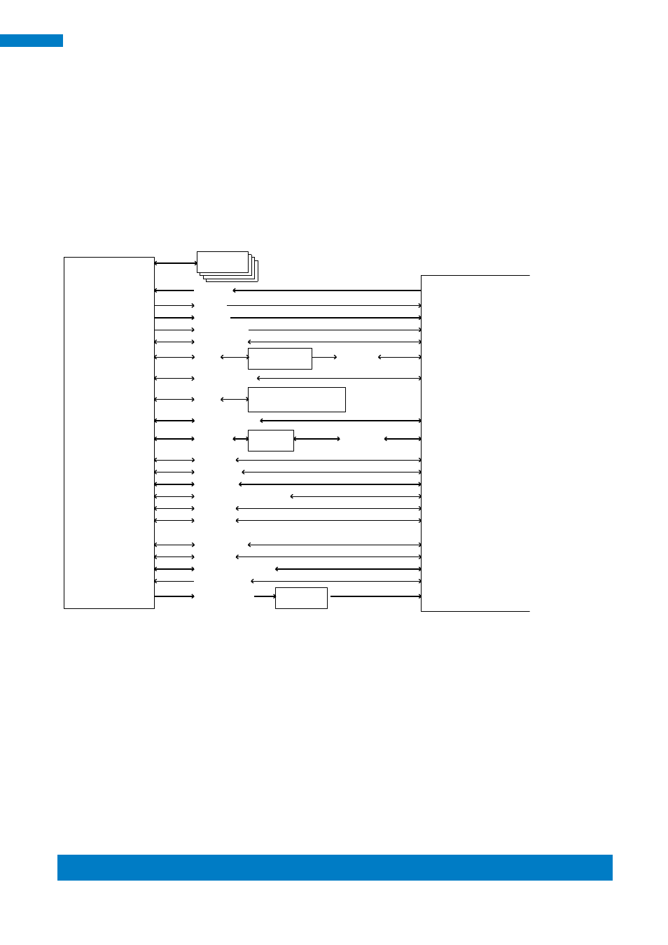
4. Carrier Board Design Guide
This Chapter mainly for advanced EE to create your own carrier boards (or products), layout suggestion
can be found inside also. for RP-100-SMC carrier board design schematic file. Please contact your sales
in advance.
4.1. Block Diagram
LVDS
DDR3
1GByte
SD2/ SDIO
HDMI
I2C x4
SPI x2
CPLD
MAX3064
24bit LCD
USB_HUB
UPD720114
USB_OTG
SPDIF x1
I2S x1
SD4/ eMMC
eMMC
KLM4G1FE3B/4GB
PHY
AR8031
USB x2
USB
CSI x1
GB_LAN
RGMII
Freescale
i.MX6
Processor
UART x4
CAN x2
Watch_DOG x1
SATA x1
PCIe x1
GPIO x12
Boot select
ULP-COM
Golden Finger
(Dual/Quad)
SD3
Advertising