7 virtex4 fpga pin allocation, Virtex4 fpga pin allocation – Sundance SMT148FX User Manual
Page 28
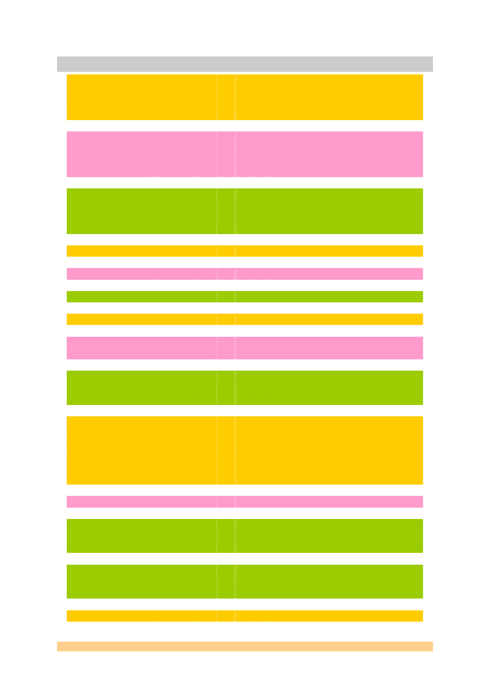
7 Virtex4 FPGA Pin Allocation
USB2 controller
CLK
1
22
SDB type interface
Data
16
Control
3
User Def
2
Firewire / OXUF922
All
29
IDE interface to OXUF922
Address
12
23
From OXUF922
Data
8
V4 Configuration data
Control
3
SHB/SDB
Data
16
2
48
2 x 16-bit data.
Control
3
WEN, REQ, ACK.
User
4
USER0-3
Clock
1
RS485
All
18
16 data and two control.
LVDS
All
56
8 groups of 7, normally routed to McBSPs via FPGA.
ComPorts
All
12
4
48
To Spartan3.
LEDs
All
12
8 x 4 matrix.
Ethernet PHY
All
12
4-bit data + 2 control for each direction.
4
RST, COMA, MDC and MDIO.
Global Bus
Address
12
4
128
Data
16
Control
4
STRB, RW, PAGE, RDY
TIM misc
TCLK
2
4
48
Config
1
IIOF,NMI
4
IACK
1
Reset
1
Individual resets to TIM sites.
Clock
3
CLKIN, H1 and H3.
RS232
All
2
Tx + Rx.
ZBT
Address
20
1
62
Data
32
Control+Clk
10
Spartan3
FPGA config
3
PROG, CCLK, DIN
Data Interface
4
CLK25, PXCLK, PXDATA, PXLOAD
Reset
1
From V4
Other
2
BDRESET, CLK50
User Manual SMT148FX
Page 28 of 48
Last Edited: 03/08/2009 11:42:00