Pin descriptions, Functional block diagram, Absolute maximum ratings – Diodes AL8400 /AL8400Q User Manual
Page 2: Package thermal data
AL8400/ AL8400Q
Document number: DS35115 Rev. 4 - 2
2 of 13
August 2012
© Diodes Incorporated
AL8400 /AL8400Q
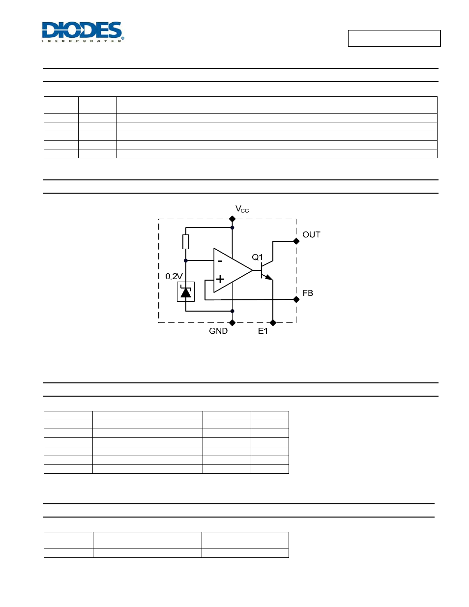
Pin Descriptions
Pin
Number
Name Function
1
E1
Emitter Connection. Connect to GND.
2
GND
Analog Ground. Ground return for reference and amplifier. Connect to E1.
3 V
CC
Supply Input. Connect a 0.47
μF ceramic capacitor close to the device from V
CC
to GND.
4
FB
Feedback Input. Regulates to 200mV nominal.
5
OUT
Output. Connect a capacitor close to device between OUT and GND. See the Applications Information section.
Functional Block Diagram
Figure 1 Block Diagram
Absolute Maximum Ratings
(@T
A
= +25°C, unless otherwise specified.)
Symbol Parameter Rating
Unit
V
CC
Supply Voltage Relative to GND
20
V
V
OUT
OUT Voltage Relative to GND
20
V
V
FB
FB Voltage Relative to GND
20
V
V
E1
E1 Voltage Relative to GND
-0.3 to+0.3
V
T
J
Operating Junction Temperature
-40 to 150
°C
T
ST
Storage Temperature
-55 to 150
°C
These are stress ratings only. Operation outside the absolute maximum ratings may cause device failure.
Operation at the absolute maximum rating for extended periods may reduce device reliability.
Package Thermal Data
Package
θ
JA
P
DIS
T
A
= +25°C, T
J
= +150°C
SOT353 400°C/W
310mW