Altera gpio timing components – Altera GPIO User Manual
Page 15
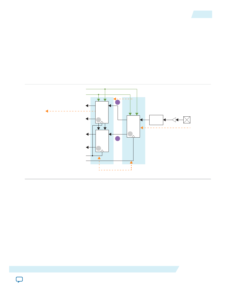
Altera GPIO Timing Components
The following paths are the timing components for Altera GPIO IP core:
• I/O interface paths (from FPGA to external receiving devices and from external transmitting devices to
FPGA)
• Core interface paths of the data and the clock (from I/O to core and from core to I/O)
• Half-rate to full-rate and full-rate to half-rate transfer paths.
Note: The TimeQuest timing analyzer treats the path inside the DDIO_IN and DDIO_OUT blocks as
black boxes.
These figures show the timing components in the Altera GPIO input, output, and output enable paths.
Figure 8: Timing Components in the Altera GPIO Input Path
PAD
ACLR_N
APRE_N
DATAOUT[0]
DATAOUT[2]
DATAOUT[1]
DATAOUT[3]
CLK_HR
CLK_FR
DDIO
IN
DDIO
IN
DDIO
IN
Delay
Element
HR
FR
B
A
1
3
2
I/O Path
Core Interface Data Path
Core Interface Clock Path
Full-rate/Half-rate Transfer Path
ug-altera_gpio
2014.08.18
Altera GPIO Timing Components
15
Altera GPIO IP Core User Guide
Altera Corporation