Output path – Altera GPIO User Manual
Page 6
Advertising
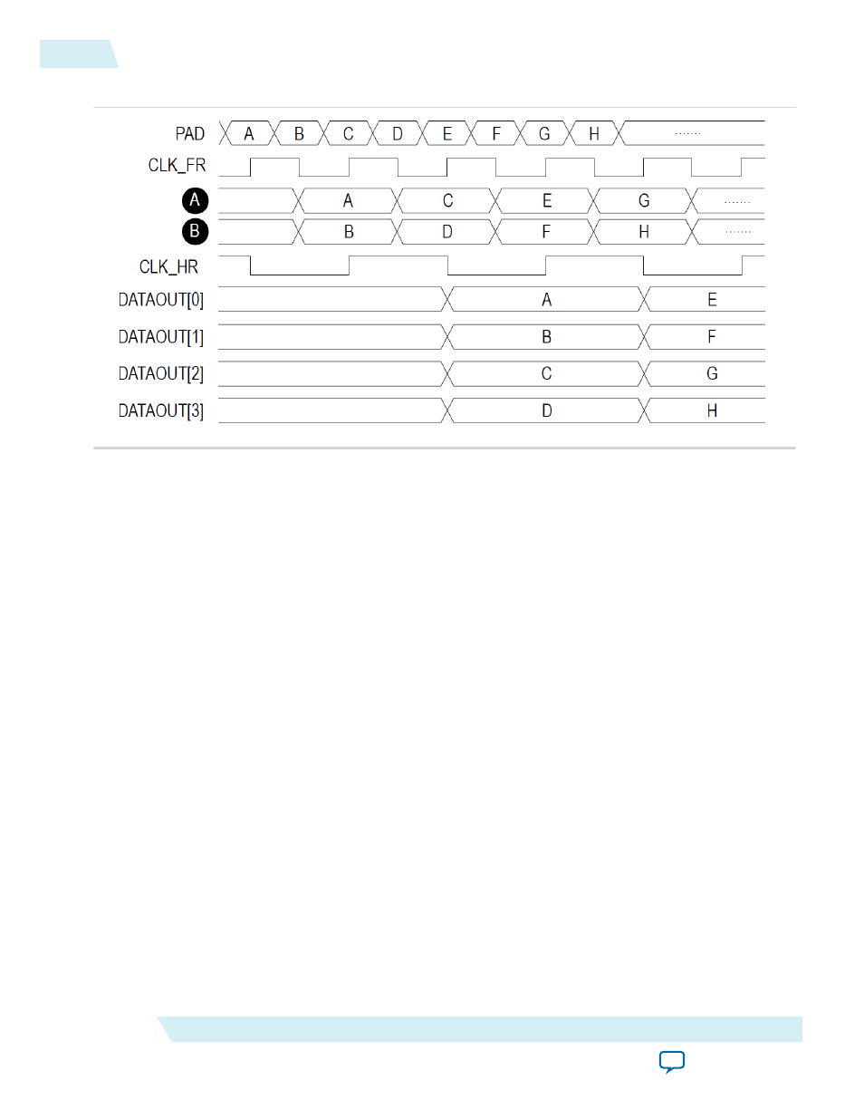
Figure 3: Input Path Waveform
The pad receives data. DDIO IN (1) (refer to
) captures data on the rising and falling edges of
CLK_FR, and sends data at SDR (refer to signals (A) and (B) in the waveform). DDIO IN (2) and DDIO
IN (3) (refer to
) halves the data rate and
DATAOUT[3:0]
presents data as a half-rate bus.
Notice how going from full-rate clock at double data rate to half-rate clock at single data rate, data rate has
been divided by four and the bus size has increased by the same ratio. The overall throughput through the
Altera GPIO IP core remained unchanged.
Output Path
The following figure shows the simplified view of a single-ended GPIO output path.
6
Output Path
ug-altera_gpio
2014.08.18
Altera Corporation
Altera GPIO IP Core User Guide
Advertising