Altera Stratix IV GX FPGA User Manual
Page 19
Chapter 4: Development Board Setup
4–3
Factory Default Switch Settings
March 2014 Altera Corporation
Stratix IV GX FPGA Development Kit User Guide
2. Set DIP switch bank (SW3) to match
3. Set DIP switch bank (SW4) to match
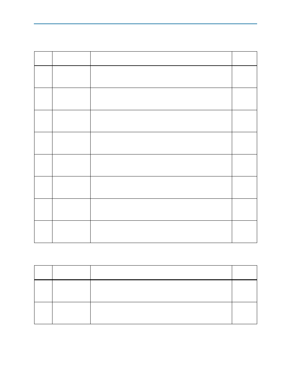
Table 4–1. SW3 Dip Switch Settings
Switch
Board
Label
Function
Default
Position
1
USER_DIPSW0
Switch 1 has the following options:
■
When on, a logic 1 is selected.
■
When off, a logic 0 is selected.
Off
2
USER_DIPSW1
Switch 2 has the following options:
■
When on, a logic 1 is selected.
■
When off, a logic 0 is selected.
Off
3
USER_DIPSW2
Switch 3 has the following options:
■
When on, a logic 1 is selected.
■
When off, a logic 0 is selected.
Off
4
USER_DIPSW3
Switch 4 has the following options:
■
When on, a logic 1 is selected.
■
When off, a logic 0 is selected.
Off
5
USER_DIPSW4
Switch 5 has the following options:
■
When on, a logic 1 is selected.
■
When off, a logic 0 is selected.
Off
6
USER_DIPSW5
Switch 6 has the following options:
■
When on, a logic 1 is selected.
■
When off, a logic 0 is selected.
Off
7
USER_DIPSW6
Switch 7 has the following options:
■
When on, a logic 1 is selected.
■
When off, a logic 0 is selected.
Off
8
USER_DIPSW7
Switch 8 has the following options:
■
When on, a logic 1 is selected.
■
When off, a logic 0 is selected.
Off
Table 4–2. SW4 Dip Switch Settings (Part 1 of 2)
Switch
Board
Label
Function
Default
Position
1
MAX_DIP
Switch 1 has the following options:
■
When on, reserved.
■
When off, reserved.
Off
2
USB_DISABLEn
Switch 2 has the following options:
■
When on, the embedded USB-Blaster is disabled.
■
When off, the embedded USB-Blaster is enabled.
Off