Using the board test system, The configure menu, The config tab – Altera Stratix IV GX FPGA User Manual
Page 28
6–4
Chapter 6: Board Test System
Using the Board Test System
Stratix IV GX FPGA Development Kit User Guide
March 2014 Altera Corporation
Using the Board Test System
This section describes each control in the Board Test System application.
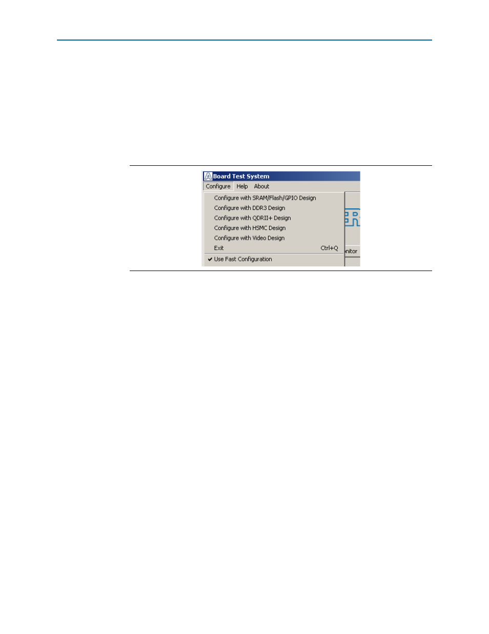
The Configure Menu
Use the Configure menu (
) to select the design you want to use. Each design
example tests different board features. Choose a design from this menu and the
corresponding tabs become active for testing.
To configure the FPGA with a test system design, perform the following steps:
1. On the Configure menu, click one of the following options to determine how to
pass data through the JTAG chain:
■
Use Fast Configuration
—Compresses the data for faster loading.
■
Use Quartus II Programmer
—Uses the standard JTAG-based configuration
method.
2. On the Configure menu, click the configure command that corresponds to the
functionality you wish to test.
3. In the dialog box that appears, click Configure or Download Start to download
the corresponding design’s SRAM Object File (.sof) to the FPGA. The download
process usually takes about a minute.
4. When configuration finishes, close the Quartus II Programmer, if using it. The
design begins running in the FPGA. The corresponding GUI application tabs that
interface with the design enable.
The Config Tab
The Config tab shows information about the board’s current configuration.
shows the Config tab. The tab displays the contents of the
MAX II registers, the JTAG chain, the board’s MAC address, the flash memory map,
and other details stored on the board.
The following sections describe the controls on the Config tab.
Board Information
The Board information controls display static information about your board.
Figure 6–2. The Configure Menu