Audio circuit pin list, Memory, Sdram schematic and pin list – Altera Cyclone II FPGA Starter Development Board User Manual
Page 25: Memory –7
Altera Corporation
Reference Manual
2–7
October 2006
Cyclone II FPGA Starter Development Board
Development Board Components
Audio Circuit Pin List
lists the FPGA pins assigned to the audio circuit.
Memory
The development board provides three types of memory:
■
An 8-MByte SDRAM
■
A 512-KByte SRAM
■
A 4-MByte flash memory
f
For information on the memory devices, refer to the
BoardDesignFiles\Datasheet
folder in the kit installation directory.
SDRAM Schematic and Pin List
shows the SDRAM interface signals.
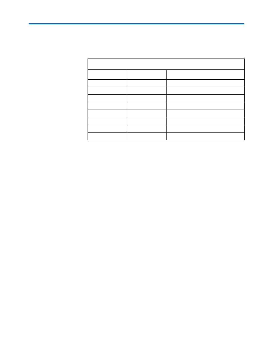
Table 2–5. Audio Circuit FPGA Pin Connections
Signal Name
FPGA Pin
Description
AUD_ADCLRCK
PIN_A6
Audio CODEC ADC LR Clock
AUD_ADCDAT
PIN_B6
Audio CODEC ADC Data
AUD_DACLRCK
PIN_A5
Audio CODEC DAC LR Clock
AUD_DACDAT
PIN_B5
Audio CODEC DAC Data
AUD_XCK
PIN_B4
Audio CODEC Chip Clock
AUD_BCLK
PIN_A4
Audio CODEC Bit-Stream Clock
I2C_SCLK
PIN_A3
I2C Data
I2C_SDAT
PIN_B3
I2C Clock