Expansion header pin list – Altera Cyclone II FPGA Starter Development Board User Manual
Page 46
Advertising
2–28
Reference Manual
Altera Corporation
Cyclone II FPGA Starter Development Board
October 2006
Development Board Components
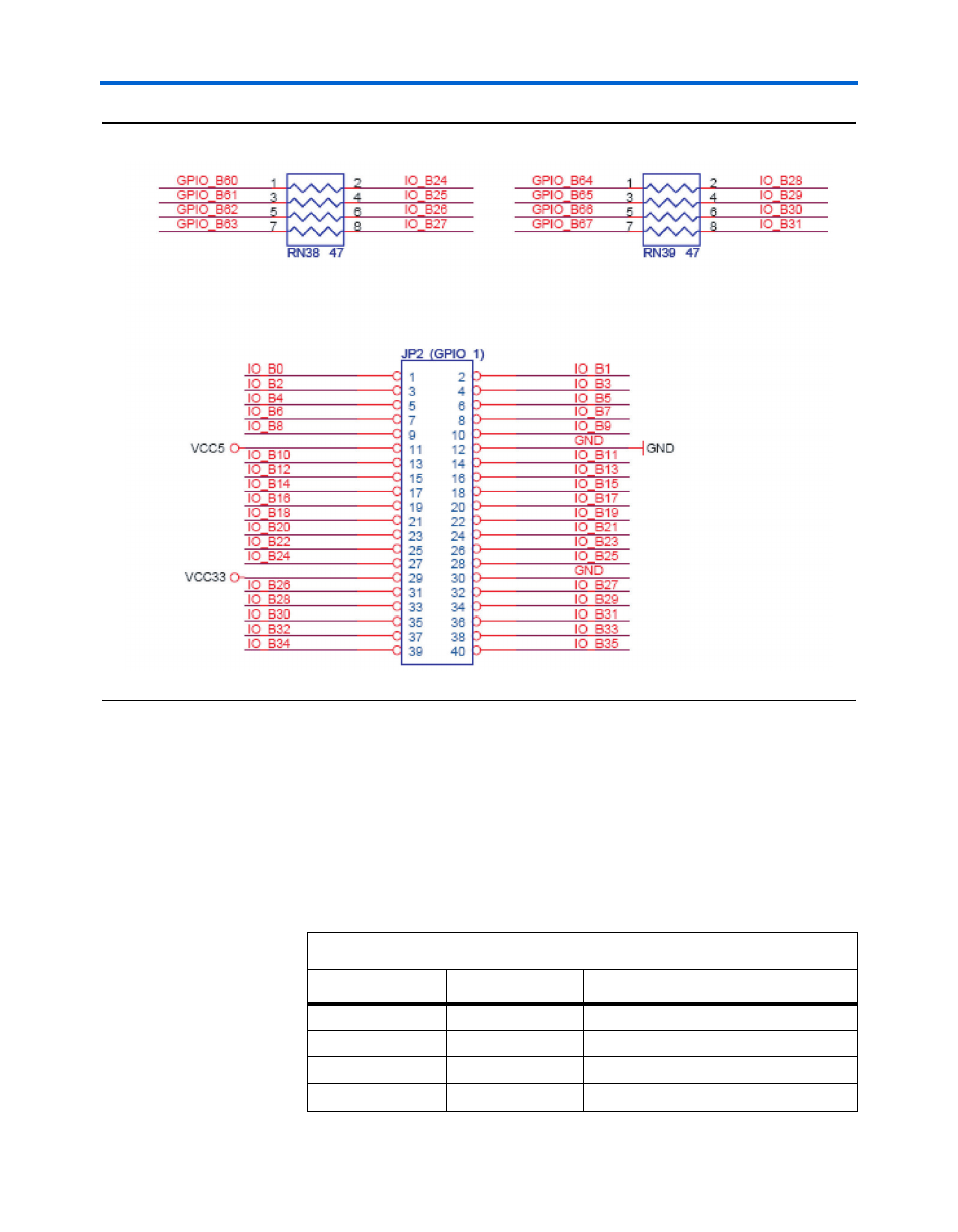
Figure 2–22. Expansion Header JP2 Schematic Diagram
As examples, the figures show the protection circuitry for 4 of the pins on
each header, but all 72 data pins include this circuitry. For complete
information, refer to the schematic found in
BoardDesignFiles\Schematic
in the kit installation directory.
Expansion Header Pin List
lists the FPGA pins assigned to the expansion headers.
Table 2–14. Expansion Header FPGA Pin Connections (Part 1 of 3)
Signal Name
FPGA Pin
Description
GPIO_0[0]
PIN_A13
GPIO Connection 0[0]
GPIO_0[1]
PIN_B13
GPIO Connection 0[1]
GPIO_0[2]
PIN_A14
GPIO Connection 0[2]
GPIO_0[3]
PIN_B14
GPIO Connection 0[3]
Advertising