Development board block diagram, Handling the board – Altera Cyclone V GX FPGA Development Board User Manual
Page 8
1–4
Chapter 1: Overview
Development Board Block Diagram
Cyclone V GX FPGA Development Board
May 2013
Altera Corporation
Reference Manual
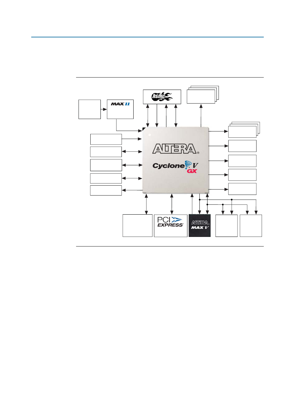
Development Board Block Diagram
shows a block diagram of the Cyclone V GX FPGA development board.
Handling the Board
When handling the board, it is important to observe the following static discharge
precaution:
c
Without proper anti-static handling, the board can be damaged. Therefore, use
anti-static handling precautions when touching the board.
Figure 1–1. Cyclone V GX FPGA Development Board Block Diagram
LVDS/Single-Ended
128-MB
DDR3
128-MB
DDR3
2x16 LCD
Push Buttons
DIP Switches
LEDs
18-MB
SSRAM
512-MB
Flash
x4 Edge
Trigger SMA Out
REFCLK SMA In
Gigabit Ethernet
PHY
Embedded
USB-Blaster II
Type-B
USB 2.0
XCVR x1
SDI TX/RX
XCVR x1
Debug Header
x1
x11
x32
x32
x4
x4
x3
ADDR x25
DATA x16
CONFIG x16
XVCR x4
x80
CLKIN x1
CLKOUT x1
XCVR x4
JTAG Chain
x1 LVPECL
Programmable
Oscillator
x4
5
6
C
L
5M2210ZF256C4N
5CGXFC7D7F31C7NES