Power down select jumper (j2, j6), D/a converter clock select jumper (j15, j17) – Altera Data Conversion HSMC User Manual
Page 10
2–4
Chapter 2: Board Components and Interfaces
Configuration, Status, and Setup Elements
Data Conversion HSMC Reference Manual
© November 2008
Altera Corporation
Power Down Select Jumper (J2, J6)
The power down configuration of the A/D converter is selectable through J2 (channel
A) or J6 (channel B).
lists the jumper settings for power down options. A/D
converters should be powered down when not used to reduce spurious noise output.
D/A Converter Clock Select Jumper (J15, J17)
lists the J15 (channel A) and J17 (channel B) jumper settings used to select
the D/A converter clock.
No Clock
—
NO_CLK_P
NO_CLK_N
Pins 1 and 3
Pins 2 and 4
Notes to
(1) Refer to the appendices for FPGA pin numbers for specific development boards.
(2) On the schematic, MUX (U9) output signal names are ADA_CLK_SEL_P and ADA_CLK_SEL_N.
(3) On the schematic, MUX (U10) output signal names are ADB_CLK_SEL_P and ADB_CLK_SEL_N.
Table 2–2. A/D Converter Clock Select Jumper (J3, J7) Settings (Part 2 of 2)
Clock Source
Board Reference
Schematic Signal Name
(1)
,
(2), (3)
A/D Converter Clock Select (J3 or J7)
Jumper Setting
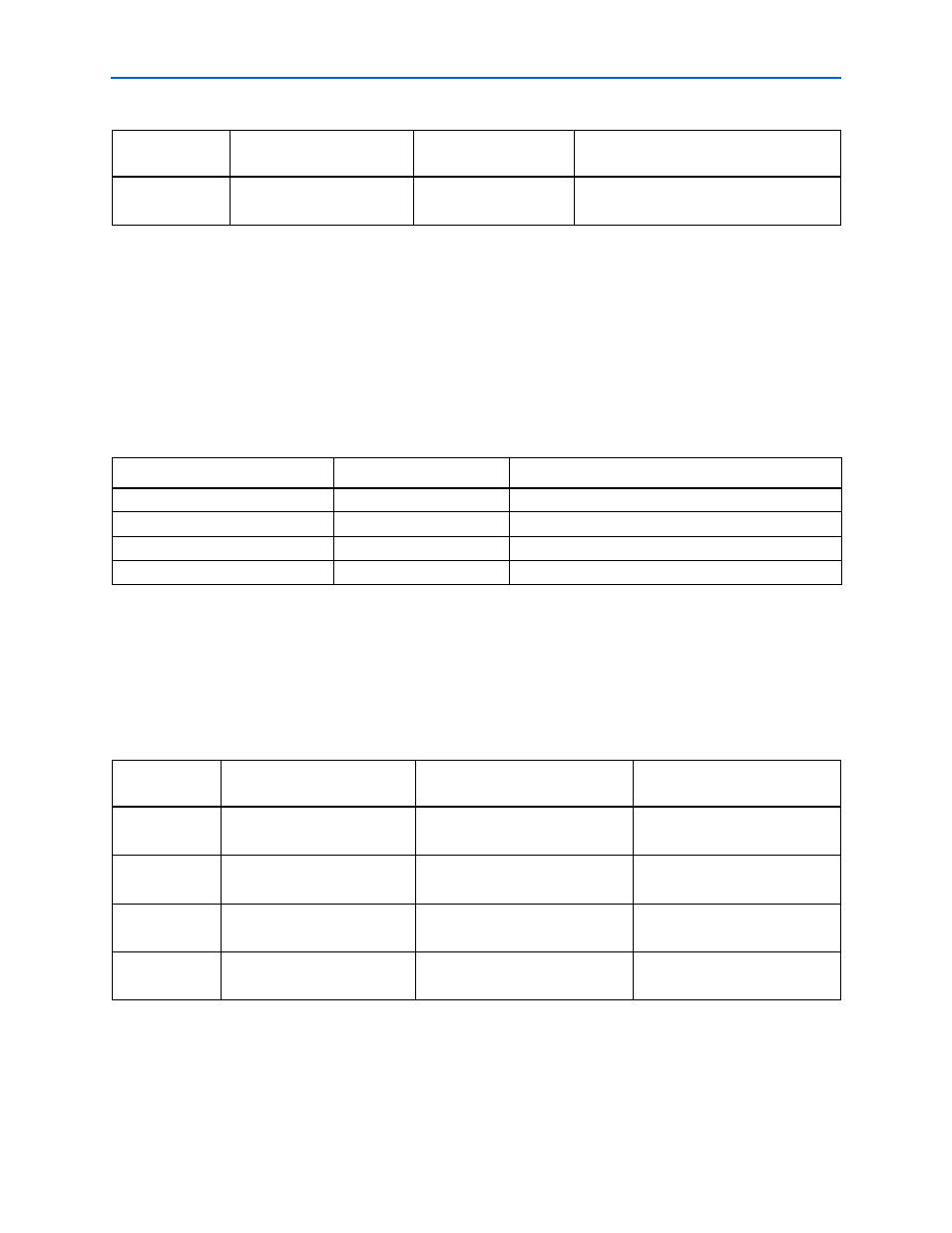
Table 2–3. Power Down Select Jumper Settings for AD9254 A/D Converter (U1, U2)
A/D Converter
Jumper Settings
Description
U1 (Channel A)
J2 Jumper OFF
A/D converter channel A in normal (operational) state
U1 (Channel A)
J2 Jumper ON
A/D converter channel A in power down
U2 (Channel B)
J6 Jumper OFF
A/D converter channel B in normal (operational) state
U2 (Channel B)
J6 Jumper ON
A/D converter channel B in power down
Note to
(1) If jumper pins are left open, A/D converter will be in normal state.
Table 2–4. D/A Converter Clock Select Jumper (J15, J17) Settings
Clock Source
Board Reference
Schematic Signal Name
D/A Converter Clock Select (J15
or J17) Jumper Setting
FPGA Clock
HSMC Connector
FPGA_CLK_A_P
FPGA_CLK_A_N
Pins 3 and 5
Pins 4 and 6
FPGA Clock
HSMC Connector
FPGA_CLK_B_P
FPGA_CLK_B_N
Pins 1 and 3
Pins 4 and 6
External Clock
External Clock Input SMA
XT_IN_P
XT_IN_N
Pins 3 and 5
Pins 2 and 4
No Clock
—
NO_CLK_P
NO_CLK_N
Pins 1 and 3
Pins 2 and 4
Notes to
(1) On the schematic, MUX (U11) output signal names are DAC_CLK_1_P and DAC_CLK_1_N.
(2) On the schematic, MUX (U12) output signal names are DAC_CLK_2_P and DAC_CLK_2_N.