Altera Data Conversion HSMC User Manual
Page 8
2–2
Chapter 2: Board Components and Interfaces
Board Overview
Data Conversion HSMC Reference Manual
© November 2008
Altera Corporation
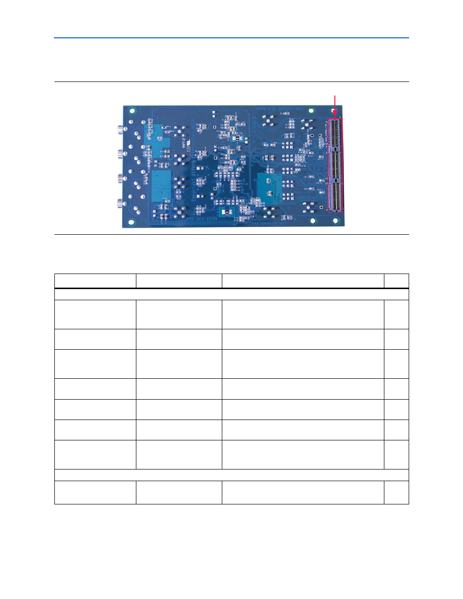
shows the back view of the Data Conversion HSMC.
lists the components and their corresponding board references.
Figure 2–2. Data Conversion HSMC—Back View
HSMC Connector (J1)
Table 2–1. Data Conversion HSMC Feature Overview (Part 1 of 2)
Board Reference
Name
Description
Page
Configuration, Status, and Setup Elements
J3 (Channel A)
J7 (Channel B)
A/D converter clock select
jumper
Controls which of the three input clock signals
(FPGA clock A, B, or the external SMA clock) is routed
to the A/D converter.
J2 (Channel A)
J6 (Channel B)
Power down select jumper
Controls whether the A/D converter operates in
power down or power up state.
J15 (Channel A)
J17 (Channel B)
D/A converter clock select
jumper
Controls which of the three input clock signals
(FPGA clock A, B, or the external SMA clock) is routed
to the D/A converter.
J11
Mode select jumper
Controls whether the D/A converter operates in dual
bus mode or interleaved mode.
J10
Gain setting select jumper
Controls whether the D/A converter channel’s gain is
set through one or two resistors.
J13
Sleep select jumper
Controls whether the D/A converter operates in
power down or power up state.
J23
External clock output select
jumper
Selects which of the four input clocks (FPGA clock A, B
or A/D converter Data Clock Output) is routed to the
SMA clock out (J28).
Clock
J26 (External Clock In-p)
J30 (External Clock In-n)
External clock input SMA
connectors
SMA connectors for a differential clock input.