3 ps, synthesizer, and d/c, p4 db25-male – Comtech EF Data CST-5005 User Manual
Page 77
CST-5005 C-Band Satellite Terminal
Theory of Operation
Rev. 1
5–7
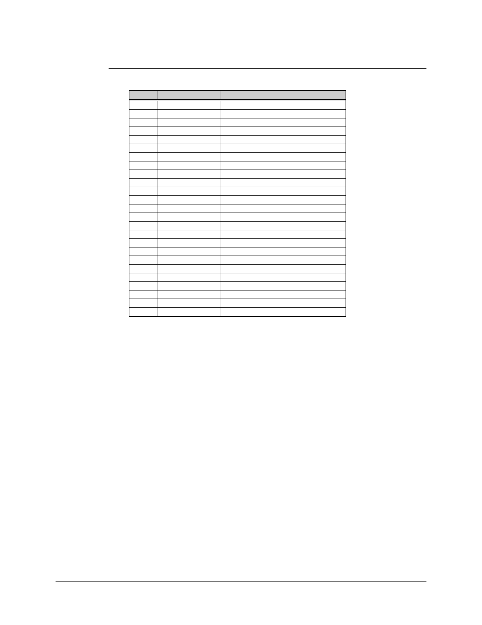
5.1.5.3 PS, Synthesizer, and D/C, P4 DB25-Male
Pin #
Name
Description
1
HPA 12V
Input, 12.5V power from PS
14
HPA 12V
Input, 12.5V power from PS
2
UC 12V
Input, 12.5V power from PS
15
M&C 12V
Input, 12.5V power from PS
3
SYN DATA
Output CMOS level, Data
16
SYN CLOCK
Output CMOS level, Clock
4
SYN EN1
Output CMOS level, Enable 1
17
SYN EN2
Output CMOS level, Enable 2
5
SYN EN3
Output CMOS level, Enable 3
18
IFLO LD
Input, Open collector, floating = fault
6
SYN LD
Input, Open collector, floating = fault
19
2ND SYN LD
Input, Open collector, floating = fault
7
OSC FLT
Input, Open collector, floating = fault
20
RNG_SW
Output, CMOS level, range select
8
DC THERM
Input, 5K thermistor tied to ground
21
SYN EN 4
Output, CMOS, Enable 4
9
DC GAIN CNTL
Output, 0 to 5V
22
SDA
Bidirectional, CMOS serial data
10
SCL
Output, CMOS serial clock
23
LNA PWR
Output, 11V power to the LNA coax
11
FREQ CNTL
Output, 0 to 10V
24
M&C GND
Ground
12
UC GND
Ground
25
HPA GND
Ground
13
HPA GND
Ground