2 monitor and control (m&c) interface connectors, 1 “system com | j1” connector – Comtech EF Data PCB-4000 User Manual
Page 23
PCB-4000 1+1 Phase Combiner
Revision 2
External Connectors
MN/PCB4000.IOM
2–3
2.2
Monitor and Control (M&C) Interface Connectors
All M&C connectors are found on the front panel of the PCCB box.
2.2.1
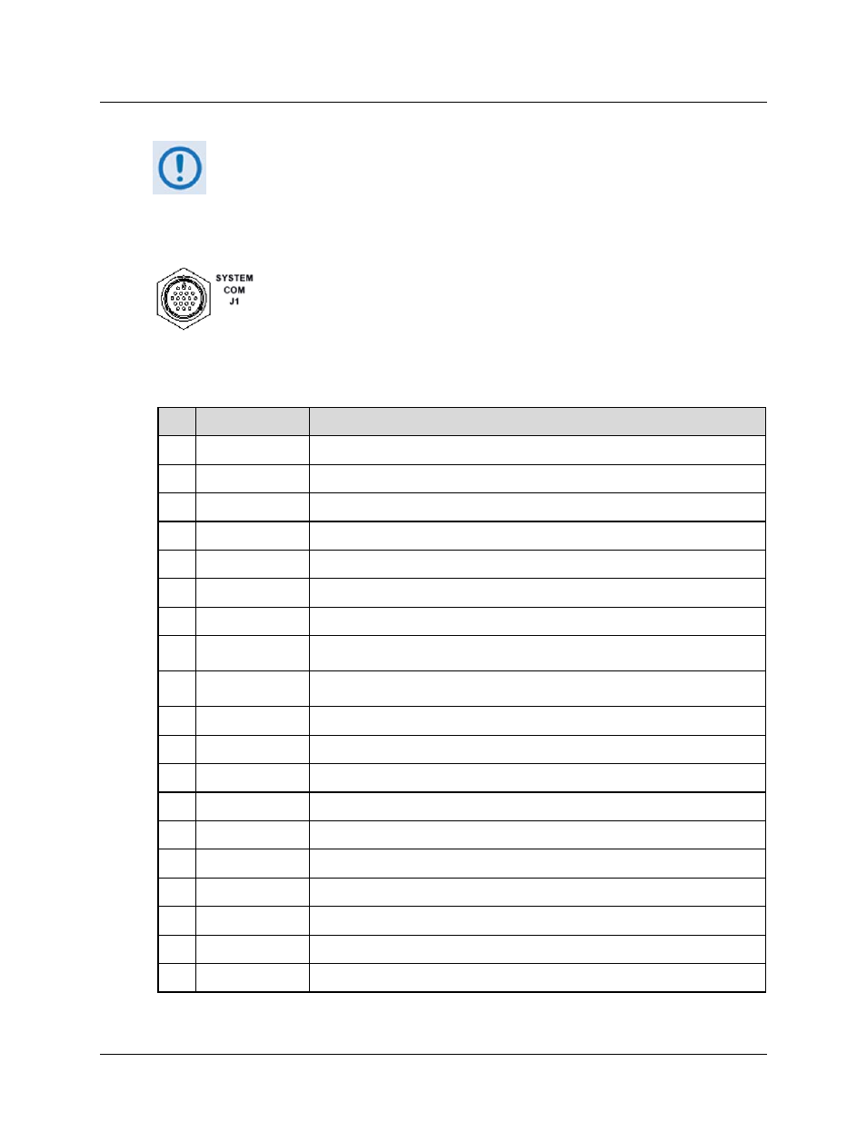
“SYSTEM COM | J1” Connector
The 19‐pin circular “SYSTEM COM | J1” connector, type MS3112E14‐19S,
serves as the primary input between the user and the PCCB for controlling and
monitoring both SSPAs.
Mating connector: ITT Cannon MS3116J14‐19P (CEFD P/N CN/MS3116J14‐19P)
Table 2-2. “SYSTEM COM | J1” Pinouts
Pin # Signal Function
Signal Name / Description
A RS485_+RX
Customer
communications
interface
B RS485_-RX
Customer
communications
interface
C RS485_+TX
Customer
communications
interface
D RS485_-TX
Customer
communications
interface
E RS232_RD
Customer
communications
interface
F
Spare
Reserved for future use
G RS232_TD
Customer
communications
interface
H
System Fault NO
When there is a summary fault in the PCB-4000, this pin (NO) will be tied to the Fault
Common pin.
J
System Fault NC
When there is not a summary fault in the PCB-4000, this pin (NC) will be tied to the Fault
Common pin.
K Fault
Common
L
SSPA 1 Fault NO
When there is a fault with SSPA 1, this pin (NO) will be tied to the Fault Common pin.
M
SSPA 1 Fault NC
When there is not a fault with SSPA 1, this pin (NC) will be tied to the Fault Common pin.
N Ground
P
SSPA 2 Fault NO
When there is a fault with SSPA 2, this pin (NO) will be tied to the Fault Common pin.
R
SSPA 2 Fault NC
When there is not a fault with SSPA 2, this pin (NC) will be tied to the Fault Common pin.
S
System Mute
SSPA will be muted if this pin is grounded
T
SSPA 3 Fault NO
( NOTE: This pin is reserved for use with 1:2 systems only.)
U
SSPA 3 Fault NC
( NOTE: This pin is reserved for use with 1:2 systems only.)
V Ground
GND