3 “sspa out 2 | j10” connector, 4 power and ground interfaces, 1 ac power – Comtech EF Data PCB-4000 User Manual
Page 27: 2 ground connector
PCB-4000 1+1 Phase Combiner
Revision 2
External Connectors
MN/PCB4000.IOM
2–7
2.3.3
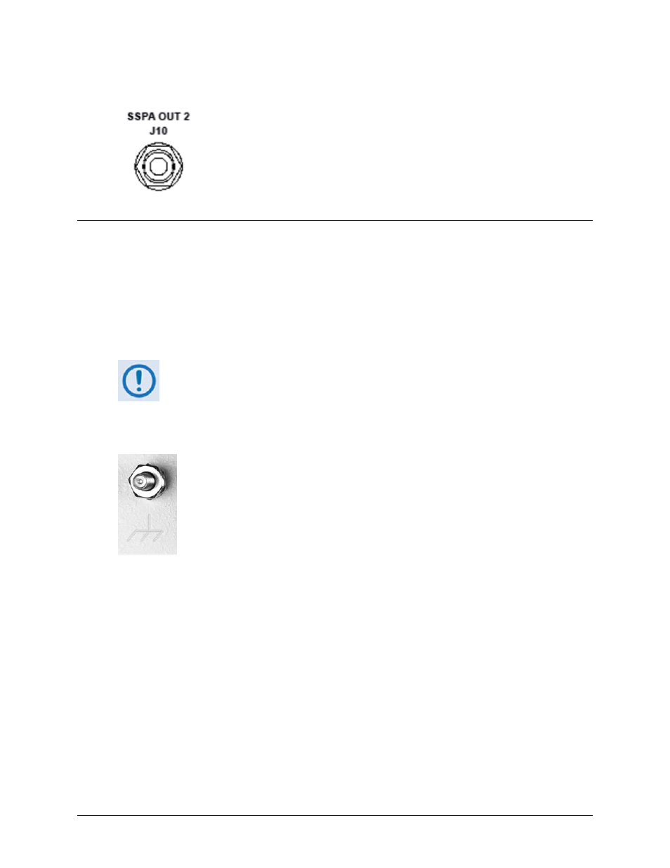
“SSPA OUT 2 | J10” Connector
The Type ‘N’ “SSPA OUT 2 | J10” connector, located on the right side panel of
the PCCB, provides the RF signal output from the PCCB to SSPA #2.
2.4
Power and Ground Interfaces
2.4.1
AC Power
The PCB‐4000 derives its power from the SSPAs. Each SSPA provides a +24V signal line via cables
interconnecting the SSPAs to the “SSPA COM 1 | J2” and “SSPA COM 2 | J3” connectors (Pin ‘R’
– see Table 2‐3 in Sect. 2.2.2). These two signals are “diode OR’ed” to provide redundancy.
Although the PCCB will turn on and function with only one SSPA powered on, the
system does not provide optimum output power unless both SSPAs are powered on.
2.4.2
Ground Connector
A #10‐32 stud is provided on the front panel of the PCCB for connecting a common
chassis ground among equipment.