Block diagram – GAI-Tronics 701-905 SmartSeries Handset/Speaker Amplifier User Manual
Page 5
Pub. 42004-685L2D
701-905
S
MART
S
ERIES
®
H
ANDSET
/S
PEAKER
A
MPLIFIER
P
AGE
4 of 15
f:\standard ioms - current release\42004 instr. manuals\42004-685l2d.doc
03/12
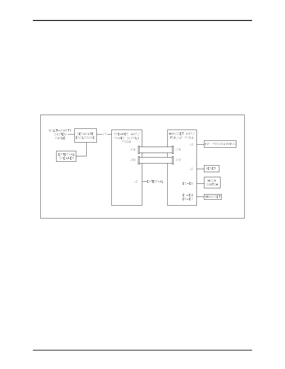
Block Diagram
The P1 connector on the back of the Speaker Amp/Power Supply PCBA plugs into a socket in an
enclosure connected to the system cable, accessing the Page/Party
®
lines and ac power. The Speaker
Amp/Power Supply PCBA contains the low voltage power supplies and the speaker amplifier circuitry.
Connector J1A and J1B on the Speaker Amp/Power Supply connects regulated +5 V dc, +/−15 V dc, and
V
RLY
voltages along with control, monitoring, and line signals to the J1A and J1B on the Handset
Amp/FSK/
P PCBA. Connector J2 of the Speaker Amp/Power Supply PCBA connects to optional
external devices.
The Handset Amp/FSK/
P PCBA has connections to the handset and the hookswitch via spade terminal
connectors E1 to E7, and it has connections to the optional front panel auxiliary connector, via J4.
Figure 3. Block Diagram
- 701-901 SmartSeries Handset / Speaker Amplifier 701-902RF SmartSeries Handset/Speaker Amplifier 701-904 SmartSeries Handset/Speaker Amplifier with Auxiliary Jack 709-901 SmartSeries Handset/Speaker Amplifier ICS 8-Channel Speaker Monitoring/Distribution Amplifier SmartSeries Handset/Speaker Amplifier with Auxiliary Jack