Pcb layout – Sundance SMT390-VP User Manual
Page 46
Advertising
Version 2.4
Page 46 of 55
SMT390-VP User Manual
Bytes 3 and 2 give the size of the FPGA: 7, 20 or 30.
Bytes 1 and 0 give the version of the FPGA firmware: 1, 2, 3, etc
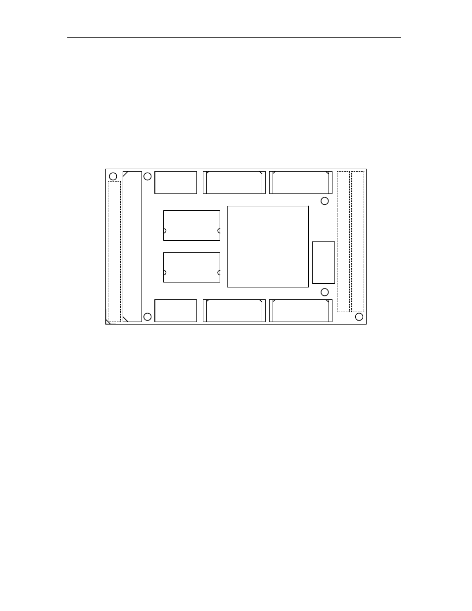
PCB Layout
The following figures show the top and bottom view of the main module, the top view
of the daughter-card and the module composition viewed from the side.
T
op
P
rim
ar
y T
IM
C
onn
ec
tor
Bot
tom
Primar
y T
IM
C
o
nnec
tor
SH
B
B
SH
B
A
RS
L
B
RS
L
A
Xil
inx
Vi
rte
x-
II Pr
o
XC
2
V
P2
0
FF
89
6 Pac
ka
ge
Global B
u
s C
onne
cto
r
Samsung
DDR266 SDRAM
Samsung
DDR266 SDRAM
D
a
u
ght
er
C
a
rd E
xpan
sion C
onnec
tor
Power
Daughter Card
Power Conn
FP
G
A
Co
n
fig
Figure 31 – Module Top View (Main Module).
Advertising