Block diagram, Fpga (xc2vp70) – Sundance SMT395E User Manual
Page 7
Advertising
Version 2.1
Page 7 of 30
SMT395Q User Manual
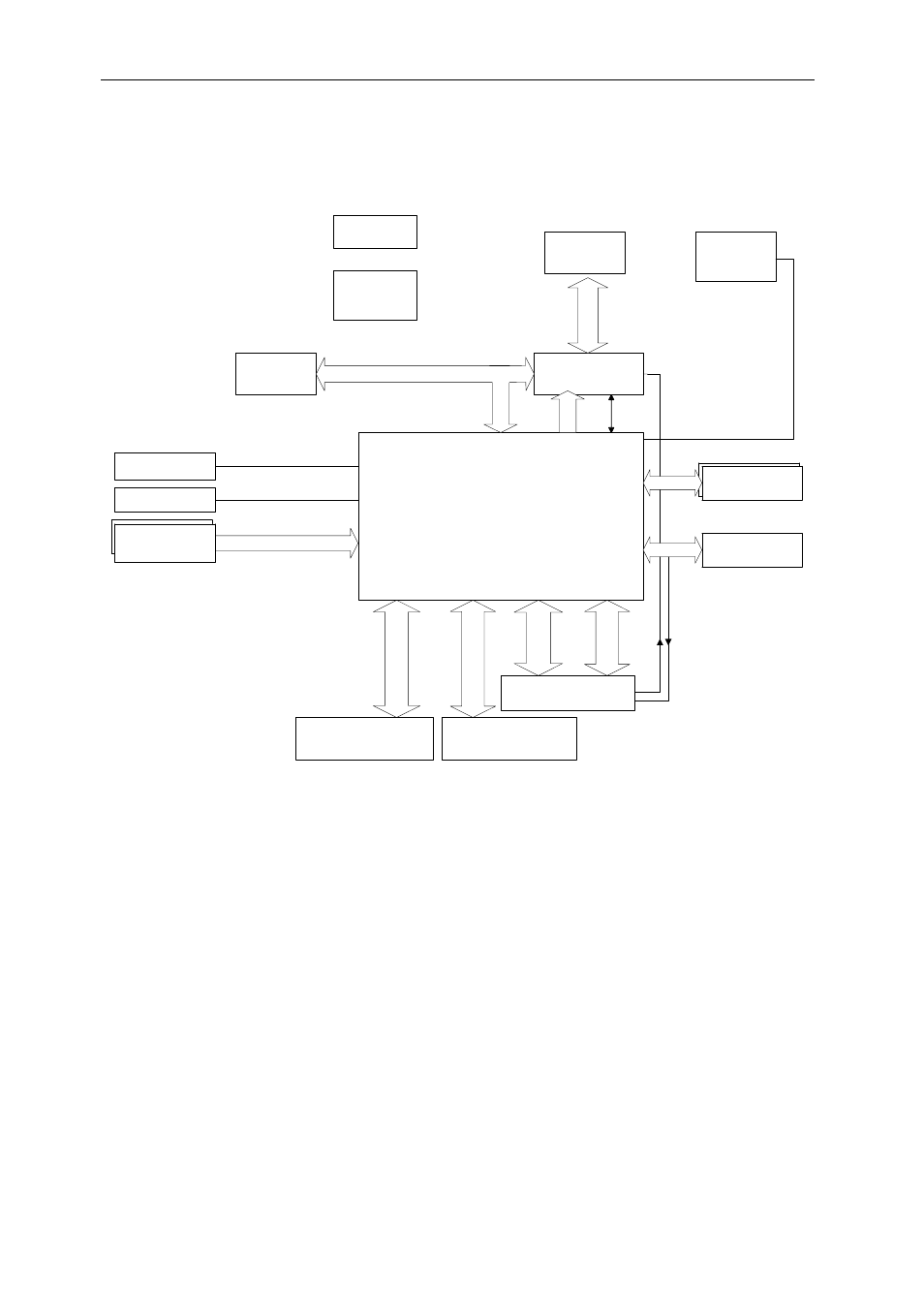
Block Diagram
120 I/O Pins; 16-bit Data
2x
Com
m
-P
o
rt
s
24
I
/O
pi
ns
Ti
m
e
r &
Co
nt
ro
l
2x
Com
m
-P
or
ts
24
I
/O
pi
ns
G
lob
al
Bus
74
I
/O
pi
ns
FPGA
(XC2VP70)
VirtexII-Pro, FF1704
996 I/O Pins
1.5V
'C6416T
DSP
JTAG Header
J1 Top Primary TIM
Connector
Comm-Port 0 & 3
J3 Global Expansion
Connector
J2 Bottom Primary TIM
Connector
Comm-Port 1 & 4
14 LEDs &
4 I/O pins
Flash (CE1)
64Mbit
Oscillators
voltage
convertors
1.5V & 1.2V
Sundance High-
Speed Bus
60-way x2
HPI
Serial
port
16
b
it
EMI
F
A
64
b
it
A
DRAM
128MBytes
Sundance RSL
x14
JTAG
chain
256MBytes
DDR memory
Power
monitoring
Advertising