Theory of operation, Module description, Figure 7: dts series transceiver block diagram – Linx Technologies TRM-915-DTS User Manual
Page 6
– –
– –
6
7
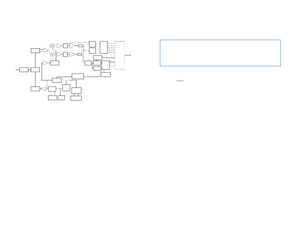
Theory of Operation
The DTS Series transceiver is a low-cost, high-performance synthesized
FSK transceiver. Its wideband operation gives it outstanding range while
still meeting regulatory requirements. Figure 7 shows a block diagram for
the module.
The DTS Series transceiver is designed for operation in the 902 to 928MHz
frequency band. The RF synthesizer contains a VCO and a low-noise
fractional-N PLL. The receive and transmit synthesizers are integrated,
enabling them to be automatically configured to achieve optimum phase
noise, modulation quality and settling time.
The transmitter output power is programmable from −4dBm to +14dBm.
The frequency deviation is optimized to deliver the highest performance
over a wide range of data rates.
The receiver incorporates highly efficient low-noise amplifiers that provide
up to –105dBm sensitivity.
An onboard controller performs the radio control and management
functions. A processor performs the higher level protocol functions and
controls the serial and hardware interfaces.
LNA
FAMP
PHASE
SHIFTER
LO_BUF
MMOD
DIVIDER
VCO
PA
CH PUMP
PFD
FAMP
VCO
TANK
LOOP
FILTER
MATCHING
NETWORK
MATCHING
NETWORK
LPF
LPF
BBAMP
LIM
LIM
OSCILLATOR
DEMOD
PATTERN
MATCHING
BBAMP
∑∆ modulator
/n
Synthesizer
FEI
BITSYNC
39MHz
XTAL
11 Bits
BARKER
DECODER
LOGIC
CONTROL
11 Bits
BARKER
ENCODER
RSSI
CONTROL
DATA
PROCESSOR
ANTENNA
SWITCH
SAW
FILTER
ANTENNA
UART /
INTERFACE
Figure 7: DTS Series Transceiver Block Diagram
Module Description
The DTS Series RF transceiver module has a Universal Asynchronous
Receiver Transmitter (UART) serial interface and is designed to create
a complete UART-to-antenna wireless solution capable of direct wire
replacement in most embedded RS-232/422/485 applications.
The module is designed to interface directly to a host UART. Three lines
are used to transfer data between the module and the host UART: TXD,
RXD, and CTS. TXD is the data output from the module. RXD is the data
input to the module. The CTS output indicates if the module is ready to
accept data. The UART interface is capable of operating in full duplex at
baud rates from 2.4 to 115.2kbps.
The module has a built-in protocol that automatically transmits the data
input on the UART. All encoding, transmitting, receiving and decoding
functions are handled by the internal processor, so no overhead is required
by an external processor.
The module can be put into a Sleep mode through serial commands. In
Sleep mode, the RF section is completely shut down and the protocol
processor is in an idle state. Once the module has been placed in the sleep
mode, it can be awakened by sending a power-up sequence through the
serial port.
If the current draw in sleep mode is too high for a particular application,
the designer can switch power to the module through a FET to turn off the
module when it is not needed. If this technique is used, the volatile registers
reset to the values in their non-volatile mirrors, so any changes from the
default will have to be reloaded.
Every module has a 48-bit MAC address that can be used by the host
application to uniquely identify each module. This MAC address can be
read through the command interface.
Note:
Although the module is capable of supporting the serial data
communications required by RS-232, RS-422, and RS-485 networks,
it is not compatible with the electrical interfaces for these types of
networks. The module has CMOS inputs and outputs and requires an
appropriate converter for the particular type of network being used.