Jtag bst architecture, Jtag pins, Jtag circuitry functional model – Altera MAX 10 JTAG User Manual
Page 4: Jtag bst architecture -1, Jtag pins -1, Jtag circuitry functional model -1
JTAG BST Architecture
2
2015.05.04
UG-M10JTAG
MAX 10 JTAG interface uses four pins,
TDI
,
TDO
,
TMS
, and
TCK
.
JTAG Pins
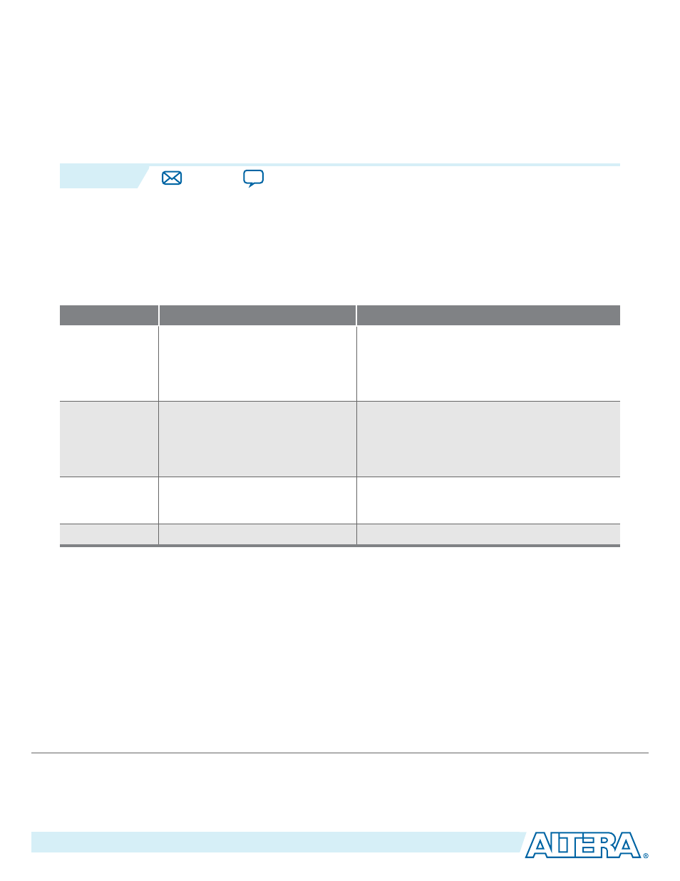
Table 2-1: JTAG Pin Descriptions
Pin
Function
Description
TDI
Serial input pin for:
• instructions
• test data
• programming data
•
TDI
is sampled on the rising edge of
TCK
•
TDI
pins have internal weak pull-up resistors.
TDO
Serial output pin for:
• instructions
• test data
• programming data
•
TDO
is sampled on the falling edge of
TCK
• The pin is tri-stated if data is not being
shifted out of the device.
TMS
Input pin that provides the control
signal to determine the transitions of
the TAP controller state machine.
•
TMS
is sampled on the rising edge of
TCK
•
TMS
pins have internal weak pull-up resistors.
TCK
The clock input to the BST circuitry.
—
All the JTAG pins are powered by the V
CCIO
1B. In JTAG mode, the I/O pins support the LVTTL/
LVCMOS 3.3-1.5V standards.
JTAG Circuitry Functional Model
The JTAG BST circuitry requires the following registers:
• Instruction register—determines which action to perform and which data register to access.
• Bypass register (1-bit long data register)—provides a minimum-length serial path between the
TDI
and
TDO
pins.
• Boundary-scan register—shift register composed of all the BSCs of the device.
©
2015 Altera Corporation. All rights reserved. ALTERA, ARRIA, CYCLONE, ENPIRION, MAX, MEGACORE, NIOS, QUARTUS and STRATIX words and logos are
trademarks of Altera Corporation and registered in the U.S. Patent and Trademark Office and in other countries. All other words and logos identified as
trademarks or service marks are the property of their respective holders as described at
www.altera.com/common/legal.html
. Altera warrants performance
of its semiconductor products to current specifications in accordance with Altera's standard warranty, but reserves the right to make changes to any
products and services at any time without notice. Altera assumes no responsibility or liability arising out of the application or use of any information,
product, or service described herein except as expressly agreed to in writing by Altera. Altera customers are advised to obtain the latest version of device
specifications before relying on any published information and before placing orders for products or services.
www.altera.com
101 Innovation Drive, San Jose, CA 95134