Boundary-scan cells in max 10 i/o pin, Boundary-scan cells in max 10 i/o pin -3 – Altera MAX 10 JTAG User Manual
Page 6
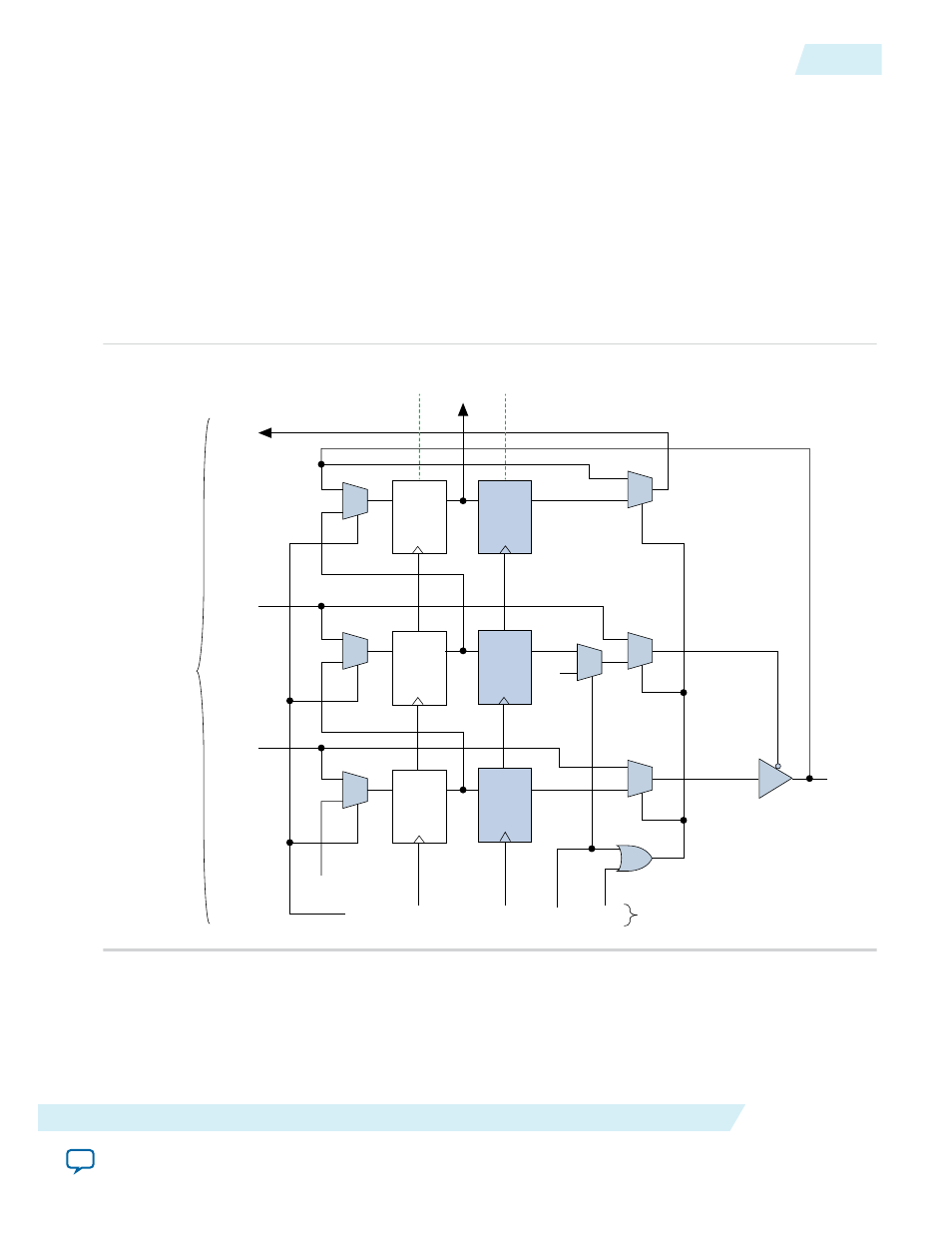
Boundary-Scan Cells in MAX 10 I/O Pin
The MAX 10 3-bit BSC contains the following registers:
• Capture registers—connect to internal device data through
OUTJ
,
OEJ
, and
PIN_IN
signals.
• Update registers—connect to external data through
PIN_OUT
and
PIN_OE
signals.
Figure 2-2: User I/O BSC with JTAG BST Circuitry for MAX 10 Devices
The TAP controller generates the global control signals internally for the JTAG BST registers,
shift
,
clock
, and
update
. The instruction register generates the
MODE
signal.
The data signal path for the boundary-scan register runs from the serial data in (
SDI
) signal to the serial
data out (
SDO
) signal. The scan register begins at the
TDI
pin and ends at the
TDO
pin of the device.
0
1
OUTPUT
OE
INPUT
INPUT
OUTPUT
OE
From or
to Device
I/O Cell
Circuitry or
Logic Array
0
1
0
1
0
1
0
1
0
1
0
1
PIN_OUT
INJ
OEJ
OUTJ
VCC
SDO
Pin
SHIFT
SDI
CLOCK
HIGHZ MODE
PIN_OE
PIN_IN
Output
Buffer
Capture
Registers
Update
Registers
Global
Signals
UPDATE
D
Q
D
Q
D
Q
D
Q
D
Q
D
Q
UG-M10JTAG
2015.05.04
Boundary-Scan Cells in MAX 10 I/O Pin
2-3
JTAG BST Architecture
Altera Corporation