Altera Double Data Rate I/O User Manual
Page 13
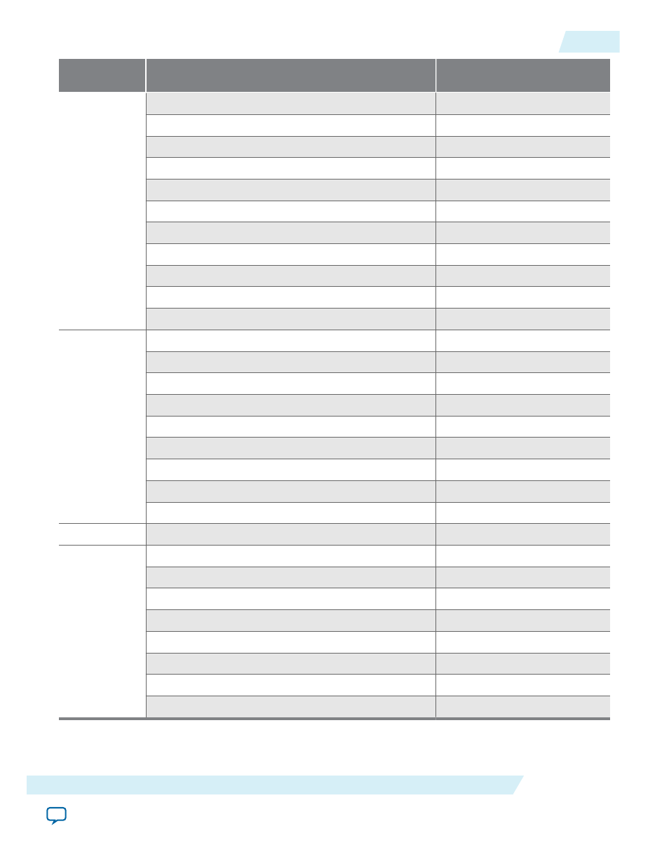
Parameter
Editor Page
Parameter
Value
3
Currently selected device family
Stratix IV
Match project/default
Turned on
Width: (bits)
8
Use ‘aclr’ port
Turned off
Use ‘aset’ port
Turned off
Not used
Turned on
Registers power up high
Turned off
Use ‘sclr’ port
Turned off
Use ‘sset’ port
Turned off
Not used
Turned on
Invert ‘padio’ port
Turned off
4
Use ‘inclocken’ and ‘outclocken’ ports
Turned off
Use output enable port
Turned on
Use ‘oe_out’ port to connect to tri-state output buffer(s)
Turned off
Register ‘oe’ port
Turned off
Delay switch-on by half a clock cycle
Turned off
Use ‘combout’ port
Turned off
Use ‘dqsundelayedout’ port
Turned off
Use ‘dataout_h’ and ‘dataout_l” ports
Turned on
Implement input registers in LEs
Turned off
5
Generate netlist
Turned off
6
Variation file
Turned on
Quartus II IP file
Turned on
Quartus II symbol file (.bsf)
Turned off
Instantiation template file
Turned on
Verilog HDL black box file (_bb.v)
Turned on
AHDL Include file (.inc)
Turned off
VHDL component declaration file (.cmp)
Turned on
PinPlanner ports file (.PPF)
Turned on
6. Click Finish.
The
ALTDDIO_BIDIR
module is now built.
UG-DDRMGAFCTN
2015.01.23
Create the ALTDDIO_BIDIR Module
13
Double Data Rate I/O (ALTDDIO_IN, ALTDDIO_OUT, and ALTDDIO_BIDIR) IP Cores User Guide
Altera Corporation