Altddio functional description, Ddr device configuration, Input configuration – Altera Double Data Rate I/O User Manual
Page 6
Parameter
Description
Use ‘dqsundelayedout’ port
Creates undelayed output from the
DQS
pins. If you
use the ALTDDIO_BIDIR IP core for your
DQS
signal in an external memory interface, you route
the undelayed
DQS
signal to the LE, in Stratix II and
Stratix devices. This option is available in Stratix,
Stratix GX, and HardCopy Stratix devices only.
Use ‘dataout_h’ and ‘dataout_l’ ports
Enables the
dataout_h
and
dataout_l
ports.
Implement input registers in LEs
Implements the input path in logic elements. This
option is available only if the
dataout_h
and
dataout_l
ports are enabled.
ALTDDIO Functional Description
DDR Device Configuration
The following sections describe how the DDR registers are configured in the Stratix series and APEX II
devices.
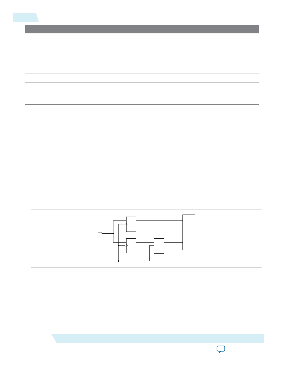
Input Configuration
When the IOE is configured as an input pin, input registers A
I
and B
I
and latch C
I
implement the input
path for DDR I/O.
Figure 1: Input DDR I/O Path Configuration for a Stratix Series or APEX II Device
This figure shows an IOE configured for DDR inputs for a Stratix series or APEX II device.
D
Q
DFF
D
Q
LA
TCH
ENA
D
Q
DFF
INPUT
datain
inclock
neg_reg_out
dataout_l
dataout_h
Input Register A
Input Register B
Latch C
Latch
Logic
Array
I
I
I
Note: On the falling edge of the clock, the negative-edge triggered register B
I
acquires the first data bit.
On the corresponding rising edge of the clock, the positive-edge triggered register A
I
acquires the
second data bit. For a successful data transfer to the logic array, the latch C
I
synchronizes the data
from register B
I
to the positive edge of the clock.
6
ALTDDIO Functional Description
UG-DDRMGAFCTN
2015.01.23
Altera Corporation
Double Data Rate I/O (ALTDDIO_IN, ALTDDIO_OUT, and ALTDDIO_BIDIR) IP Cores User Guide