Latency timer configuration register (debug tab) – Altera PCI Development Kit, Cyclone II Edition Getting Started User Manual
Page 21
Advertising
Altera Corporation
Core Version a.b.c variable
2–11
May 2005
PCI Development Kit, Cyclone II Edition Getting Started User Guide
Getting Started
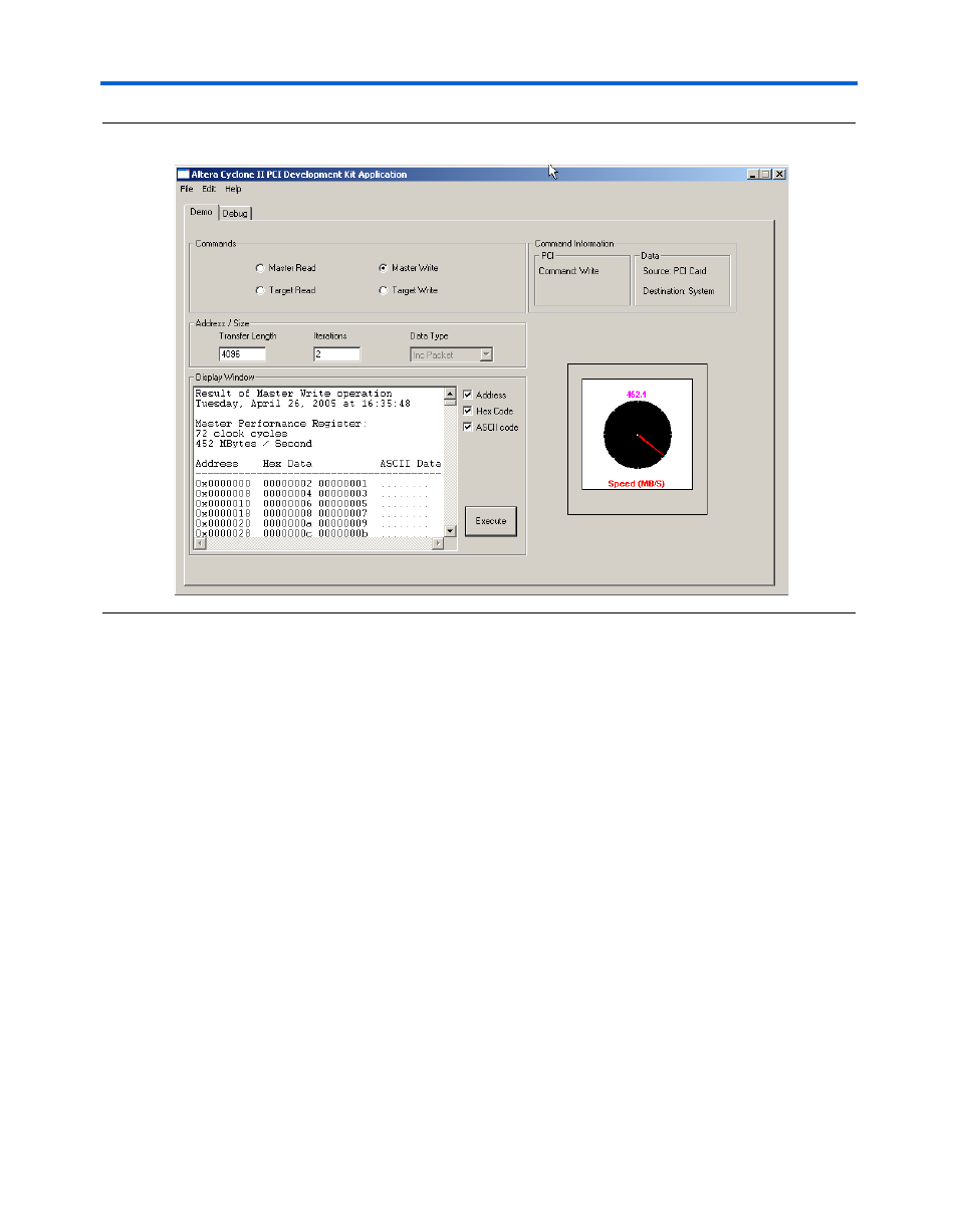
Figure 2–5. PCI Master Write Transaction (Demo Tab)
Latency Timer Configuration Register (Debug Tab)
In this example, the data source is the PCI board and the destination is the
system memory, employing a user-configured value for the latency timer.
You can verify this setup in the Command Information section of the kit’s
application.
1.
Click the Debug tab.
2.
Select Master Write from the Commands box.
3.
Keep the Address Offset setting of 0x0000000.
4.
Keep the following values in the Address/Size box:
●
Transfer Length: 4,096
●
Iterations: 2
5.
In the Configuration Registers list, select Lat Timer.
Advertising