Altera Arria V SoC Development Board User Manual
Page 12
2–4
Chapter 2: Board Components
Board Overview
July 2014
Altera Corporation
Reference Manual
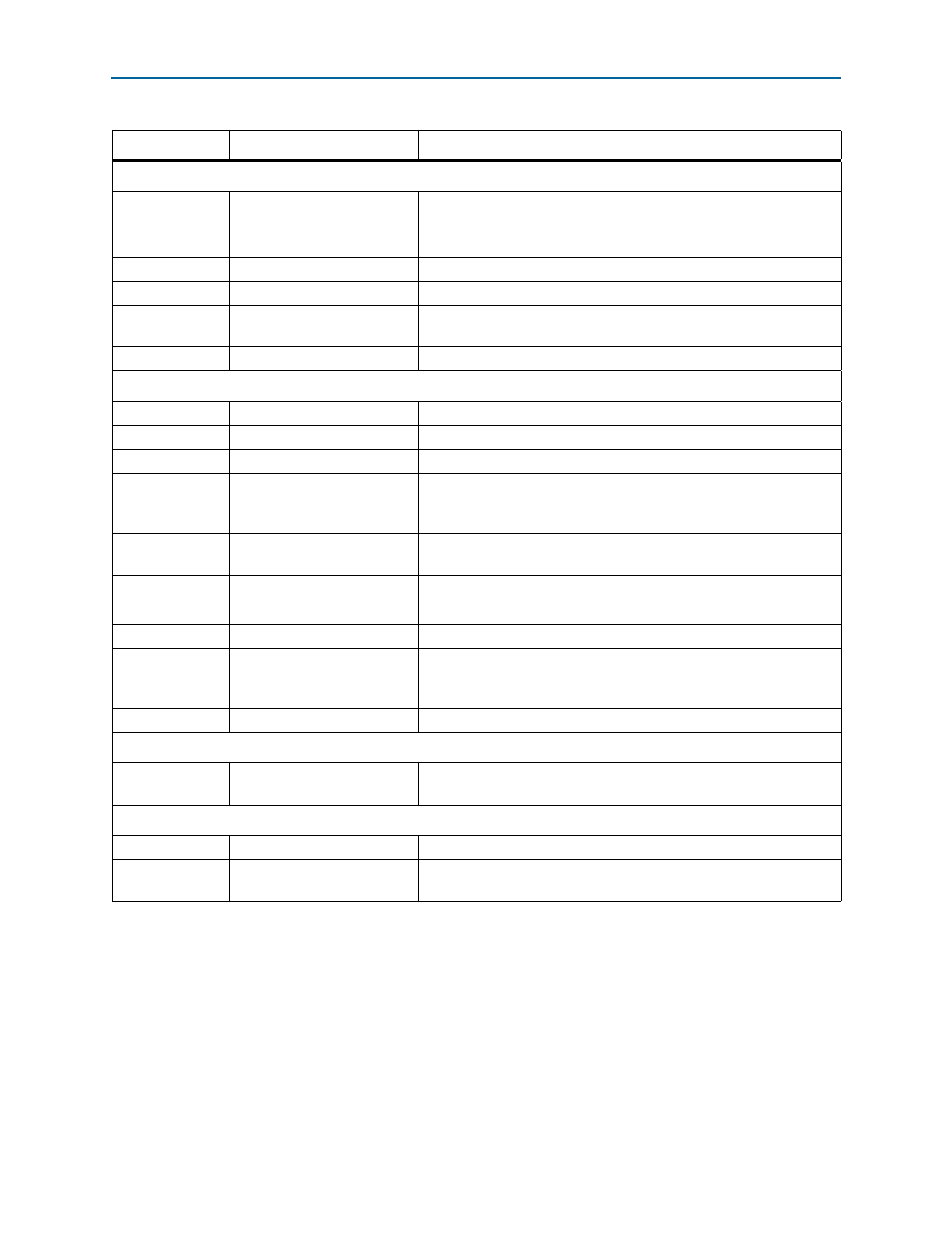
Memory Devices
U29, U37, U43,
U49,
U38, U44, U51
DDR3 SDRAM
Four 128-MB DDR3 SDRAM with a 16-bit data bus for the FPGA and
three 128-MB DDR3 SDRAM with a 16-bit data plus ECC bus for the
HPS.
U19
QSPI flash
1-Gb serial NOR flash with 4-bit data bus.
U28
EPCQ flash
U13
Synchronous flash
128-Mb synchronous flash devices with a 16-bit data bus for
non-volatile memory.
U31
I
2
C EEPROM
32-Kb I
2
C serial EEPROM.
Communication Ports
J42
PCI Express socket
PCI Express Gen1/Gen2 ×4 socket.
J4, J26
FMC port
Two FMC ports
J43, J44
SFP+ port
Two SFP+ ports
U7, J13
Gigabit Ethernet port
RJ-45 connectors which provides a 10/100/1000 Ethernet connection
via a Micrel KSZ9021RN PHY and the FPGA-based Altera Triple Speed
Ethernet MegaCore function in RGMII mode (for HPS).
U55, J47, J48
Dual Ethernet port
RJ-45 connector which provides a 10/100 Ethernet connection via a
Renesas uPD60620 PHY in MII mode (for FPGA).
J22, U25
J27, U36
USB-UART ports
USB connector with USB-to-UART bridge for serial UART interface.
J1, U4
USB OTG port
USB 2.0 on-the-go interface.
U11
Real-time clock
DS1339 device with built-in power sense circuit that detects power
failures and automatically switches to backup battery supply,
maintaining time.
J5
Micro SD card socket
Micro SD card interface with 4-bit data line.
Video and Display Ports
J29
Character LCD
Connector that interfaces to a provided 16 character × 2 line LCD
module along with two standoffs.
Power Supply
J34
DC input jack
Accepts 16-V DC power supply.
SW5
Power switch
Switch to power on or off the board when power is supplied from the
DC input jack.
Table 2–1. Board Components (Part 3 of 3)
Board Reference
Type
Description