Fpga configuration, Fpga programming over on-board usb-blaster ii, Fpga configuration –10 – Altera Arria V SoC Development Board User Manual
Page 18: Fpga programming over on-board usb-blaster ii –10
2–10
Chapter 2: Board Components
FPGA Configuration
July 2014
Altera Corporation
Reference Manual
FPGA Configuration
This section describes the FPGA, flash memory, and MAX V CPLD 5M2210 System
Controller device programming methods supported by the Arria V SoC development
board.
The Arria V SoC development board supports the following configuration methods:
■
JTAG
■
On-board USB-Blaster II is the default method for configuring the FPGA using
the Quartus II Programmer in JTAG mode with the supplied USB cable.
■
External Mictor connector for configuring the HPS using the ARM DS-5 Altera
Edition software and DSTREAM or Lauterbach cables.
■
External USB-Blaster for configuring the FPGA when you connect the external
USB-Blaster to the JTAG header (J35).
■
Flash memory download for configuring the FPGA using stored images from the
flash memory on either power-up or pressing the configure push button (S12).
FPGA Programming over On-Board USB-Blaster II
This configuration method implements a mini-USB connector (J50), a USB 2.0 PHY
device (U61), and an Altera MAX II CPLD EPM570GF100I5N (U56) to allow FPGA
configuration using a USB cable. This USB cable connects directly between the USB
connector on the board and a USB port on a PC running the Quartus II software.
The on-board USB-Blaster II in the MAX II CPLD EPM570GF100I5N normally masters
the JTAG chain. The on-board USB-Blaster II shares the pins with the external header.
and is automatically disabled when you connect an external USB-Blaster to the JTAG
chain through the JTAG header (J35). In addition to JTAG interface, the on-board USB-
Blaster II has trace capabilities for HPS debug purposes. The trace interface from the
HPS routes to the on-board USB-Blaster II connection pins through the FPGA.
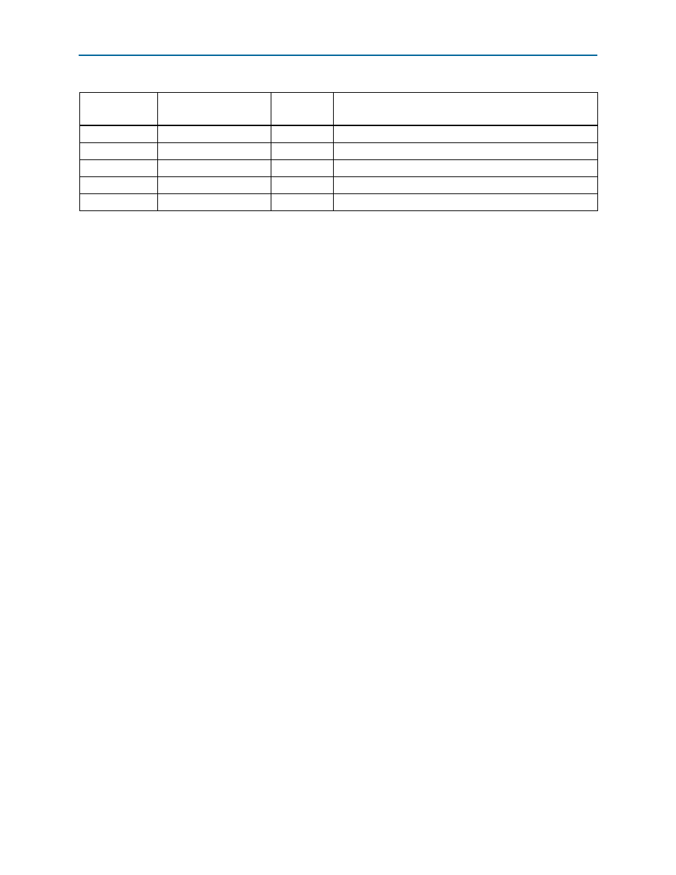
P9
USB_CFG9
1.5-V
On-board USB-Blaster II interface (reserved for future use)
M8
USB_CFG10
1.5-V
On-board USB-Blaster II interface (reserved for future use)
T10
USB_CFG11
1.5-V
On-board USB-Blaster II interface (reserved for future use)
A13
USB_FPGA_RESET
2.5-V
On-board USB-Blaster II interface FPGA reset
A11
USB_RESET
2.5-V
On-board USB-Blaster II interface reset
Table 2–3. MAX V CPLD System Controller Device Pin-Out (Part 5 of 5)
Board
Reference (U27)
Schematic Signal Name
I/O Standard
Description